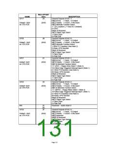
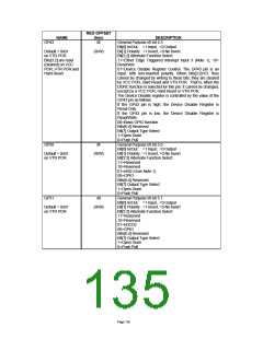
REG OFFSET
NAME
(hex)
3E
DESCRIPTION
General Purpose I/0 bit 4.3
GP43
Bit[0] In/Out : =1 Input, =0 Output
Bit[1] Polarity : =1 Invert, =0 No Invert
Bit[3:2] Alternate Function Select
11=Either Edge Triggered Interrupt Input 3 (Note 1), 10=
Reserved
01=Device Disable Register Control. The GP43 pin is an
input, with non-inverted polarity. When bits[3:2]=01, they
cannot be changed by writing to these bits; they are cleared
by VCC POR, Hard Reset and VTR POR. That is, when the
DDRC function is selected for this pin, it cannot be changed,
except by a VCC POR, Hard Reset or VTR POR.
The Device Disable register is controlled by the value of the
GP43 pin as follows:
Default = 0x01
on VTR POR
Bits[3:2] are reset
(cleared) on VCC
POR, VTR POR and
Hard Reset
(R/W)
If the GP43 pin is high, the Device Disable Register is
Read-Only.
If the GP43 pin is low, the Device Disable Register is
Read/Write.
00=Basic GPIO function
Bits[6:4] Reserved
Bit[7] Output Type Select
1=Open Drain
0=Push Pull
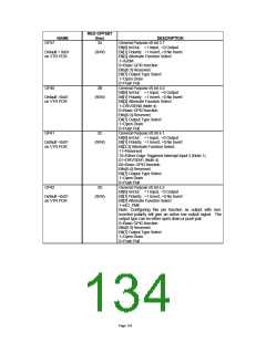
GP50
3F
General Purpose I/0 bit 5.0
Bit[0] In/Out : =1 Input, =0 Output
Bit[1] Polarity : =1 Invert, =0 No Invert
Bit[3:2] Alternate Function Select
11=Reserved
Default = 0x01
on VTR POR
(R/W)
10=Reserved
01=nRI2 (User Note 1)
00=GPIO
Bits[6:4] Reserved
Bit[7] Output Type Select
1=Open Drain
0=Push Pull
GP51
40
General Purpose I/0 bit 5.1
Bit[0] In/Out : =1 Input, =0 Output
Bit[1] Polarity : =1 Invert, =0 No Invert
Bit[3:2] Alternate Function Select
11=Reserved
Default = 0x01
on VTR POR
(R/W)
10=Reserved
01=nDCD2
00=GPIO
Bits[6:4] Reserved
Bit[7] Output Type Select
1=Open Drain
0=Push Pull
Page 135

 SMSC [ SMSC CORPORATION ]