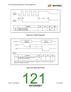
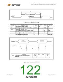
Non-PCI Single-Chip Full Duplex Ethernet Controller with Magic Packet
Chapter 13 LAN91C96 Revisions
DATE
PAGE(S)
SECTION/FIGURE/ENTRY
Ordering Information
CORRECTION
REVISED
2
92
Added lead-free ordering information
Modified Supply Current in power down
09/10/04
08/11/04
DC Electrical Characteristics
mode
65
50
Theory of Operation (Magic Packet
Support section)
I/O Space – Bank1 Offset 2
Modified descriptions of Magic Packet
Support
08/11/04
09/30/02
09/17/02
07/01/02
07/01/02
Modified I/O base address 300h
decoding
124~125
16
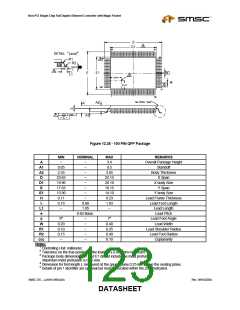
Fig.12.28100 pin QFP Package;
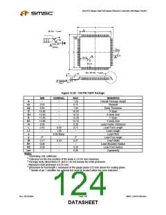
Fig.12.28100 Pin TQFP Package;
Updated Pin Package diagrams
Add description of RBIAS pin
Chapter 4 Description of Pin
Functions
58
IO Space Bank 2 Offset 2 – Interrupt
Modified the description of Interrupt
Registers
61
59
67
Figure 7.1 – Interrupt Structure
Bank 3 Offset A – Revision Register
Modified Interrupt Structure Figure
Changed the REV ID to 9
Modified the flow chart
07/01/02
07/01/02
07/01/02
8.1, 8.2 Typical Flow of Events for
Transmit
1
Title and document
Non-PCI replaces ISA/PCMCIA in title.
Local Bus replaces ISA throughout
document.
04/15/02
70
37
37
Figure 8.1 – Interrupt Service Routine Figure has been updated.
04/15/02
07/27/01
07/27/01
Figure 6.1 – Data Frame Format
Data area in ram
Max Offset changed to 1534 from 1536
Number of Bytes in Data Area changed
to 1531 from 2034
25
108
Figure 7
DC Electrical Characteristics
Update Figure 7
07/27/01
07/27/01
Update 3.3V Characteristic Numbers
replace TBD
80
37
37
Figure 15
Figure 6.1 – Data Frame Format
Data area in ram
Updated figure 15
Max Offset changed to 1534 from 1536
03/21/01
07/27/01
07/27/01
Number of Bytes in Data Area changed
to 1531 from 2034
25
108
Figure 7
DC Electrical Characteristics
Update Figure 7
07/27/01
07/27/01
Update 3.3V Characteristic Numbers
replace TBD
80
55
Figure 15
Updated figure 15
03/21/01
07/18/00
I/O Space – Bank 2/ Top of RX FIFO
MMU Commands changed from 3, 4 to
Packet Number
6, 8
See italicized text
20
92
99
Buffer Symbols
DC Electrical Characteristics
Timing Diagrams
See italicized text
Updated table – see italicized text
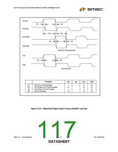
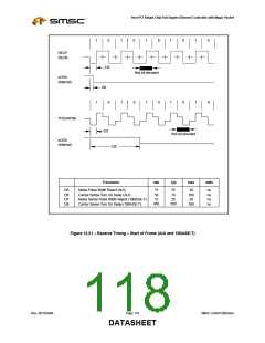
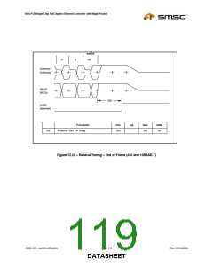
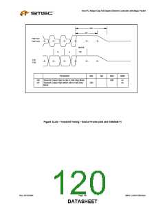
Figures: 20-23, 25, 29, 31-33, 35-37
06/29/00
06/29/00
06/29/00
SMSC DS – LAN91C965v&3v
Page 125
Rev. 09/10/2004
DATASHEET

 SMSC [ SMSC CORPORATION ]