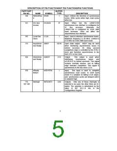
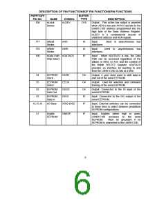
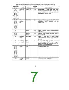
DESCRIPTION OF PIN FUNCTIONSOF PIN FUNCTIONSPIN FUNCTIONS
PQFP/TQFP
PIN NO.
BUFFER
TYPE
NAME
SYMBOL
DESCRIPTION
1
nLink Status nLNK
IP
Input. General purpose input port used to
convey LINK status (EPHSR bit 14).
Independent of port selection (MIISEL=X).
195
6
nFullstep
MII Select
nFSTEP
O4
O4
Output. Non volatile output pin. Driven by
inverse of FULLSTEP (CONFIG bit 10).
Independent of port selection (MII SEL=X).
MIISEL
Output. Non volatile output pin. Driven by
MII SELECT (CONFIG bit 15). High
indicates the MII port is selected, low
indicates the 10 Mbps ENDEC is selected.
194
30
AUI Select
AUISEL
O4
O4
IP
Output. Non volatile output pin. Driven by
AUI SELECT (CONFIG bit 8). Independent
of port selection (MIISEL=X).
Transmit
Enable 100
Mbps
TXEN100
Output to MII PHY. Envelope to 100 Mbps
transmission. This pin stays low if MIISEL is
low.
19
Carrier 100 CRS100
Mbps
Input from MII PHY. Envelope of packet
reception used for deferral and backoff
purposes. This pin is ignored when MIISEL
is low.
12
18
Receive
Data Valid
RX_DV
ID
ID
Input from MII PHY. Envelope of data valid
reception. Used for receive data framing.
This pin is ignored when MIISEL is low.
Collision
Detect 100
Mbps
COL100
Input from MII PHY. Collision detection
input. This pin is ignored when MIISEL is
low.
25,26,
28,29
Transmit
Data
TXD0-TXD3
TX25
O4
IP
Outputs. Transmit Data nibble to MII PHY.
9
Transmit
Clock
Input. Transmit clock input from MII. Nibble
rate clock (25 MHz). This pin is ignored
when MIISEL is low.
17
Receive
Clock
RX25
IP
I
Input. Receive clock input from MII PHY.
Nibble rate clock. This pin is ignored when
MIISEL is low.
20,21,
22,24
Receive
Data
RXD0-
RXD3
Inputs. Received Data nibble from MII PHY.
These pins are ignored when MIISEL is low.
9

 SMSC [ SMSC CORPORATION ]