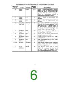
DESCRIPTION OF PIN FUNCTIONSOF PIN FUNCTIONSPIN FUNCTIONS
PQFP/TQFP
PIN NO.
BUFFER
TYPE
NAME
SYMBOL
MDI
DESCRIPTION
198
Manage-
ment Data
Input
IP
MII management data input.
196
Manage-
ment Data
Output
MDO
O4
MII management data output.
MII management clock.
192
11
Manage-
ment Clock
MCLK
O4
ID
Receive
Error
RX_ER
Input. Indicates a code error detected by
PHY. Used by the LAN91C100 to discard
the packet being received.
The error
indication reported for this event is the same
as a bad CRC (Receive Status Word bit 13).
This pin is ignored when MIISEL is low.
204
7
Bias
Resistor
RBIAS
Analog
Input
A bias resistor is connected between this pin
and ground. Nominal value is TBD.
nChip
Select
Output
nCSOUT
O4
Output. Chip Select provided for mapping
of PHY functions into LAN91C100 decoded
space. Active on accesses to LAN91C100's
eight lower addresses when the BANK
SELECTED is 7.
10

 SMSC [ SMSC CORPORATION ]