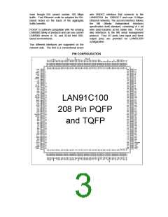
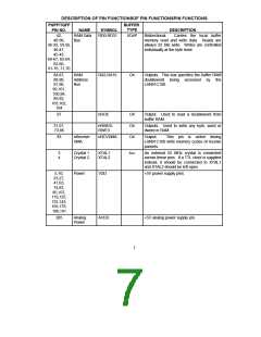
DESCRIPTION OF PIN FUNCTIONSOF PIN FUNCTIONSPIN FUNCTIONS
PQFP/TQFP
PIN NO.
BUFFER
TYPE
NAME
SYMBOL
DESCRIPTION
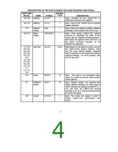
42,
40-38,
36-33, 59,56,
49-47,
RAM Data
Bus
RD0-RD31
I/O4P
Bidirectional.
Carries the local buffer
memory read and write data. Reads are
always 32 bits wide. Writes are controlled
individually at the byte level.
45-43,
69-67, 65,64,
62-60,
81-76, 71,70
84,87,
88,90,
91,96,
99,101,
100,98,
89,92,
103,102,
104
RAM
Address
Bus
RA2-RA16
O4
Outputs. This bus specifies the buffer RAM
doubleword being accessed by the
LAN91C100.
97
nROE
O4
O4
O4
Output. Used to read a doubleword from
buffer RAM.
31,57,
73,86
nRWE0-
RWE3
Outputs. Used to write any byte, word or
dword in RAM.
93
nReceive
DMA
nRCVDMA
Output.
This pin is active during
LAN91C100 write memory cycles of receive
packets.
3
4
Crystal 1
Crystal 2
XTAL1
XTAL2
ICLK
An external 25 MHz crystal is connected
across these pins. If a TTL clock is supplied
instead, it should be connected to XTAL1
and XTAL2 should be left open.
5,10,
23,27,
Power
VDD
+5V power supply pins.
41,63,
74,83,
85,107,
119,125,
132,143,
165,179,
186,191
205
Analog
Power
AVDD
+5V analog power supply pin.
7

 SMSC [ SMSC CORPORATION ]