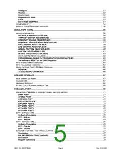
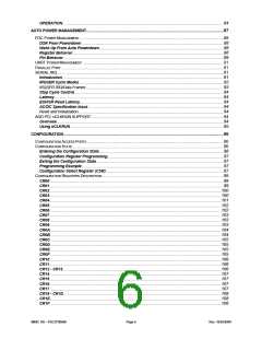
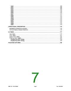
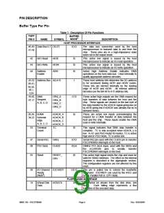
PIN DESCRIPTION
Buffer Type Per Pin
Table 1 - Description Of Pin Functions
TQFP
PIN #
BUFFER
MODE6
NAME
SYMBOL
DESCRIPTION
HOST PROCESSOR INTERFACE
46-49 Data Bus 0-7 D0-D7
51-54
IO12
The data bus connection used by the host
microprocessor to transmit data to and from the
chip. These pins are in a high-impedance state
when not in the output mode.
42
43
44
nI/O Read
nI/O Write
nIOR
nIOW
AEN
IS
IS
IS
This active low signal is issued by the host
microprocessor to indicate an I/O read operation.
This active low signal is issued by the host
microprocessor to indicate an I/O write operation.
Active high Address Enable indicates DMA
operations on the host data bus. Used internally to
qualify appropriate address decodes.
Address
Enable
26-32 Address Bus A0-A15
39-41,
I
These host address bits determine the I/O address
to be accessed during nIOR and nIOW cycles.
These bits are latched internally by the leading
edge of nIOR and nIOW. All internal address
decodes use the full A0 to A15 address bits.
95,35,
36,1,
3,25
19,50, DMA
Request
A, B, C, D
DRQ_A
DRQ_B
DRQ_C
DRQ_D
O12
These active high outputs are the DMA request for
byte transfers of data between the host and the
chip. These signals are cleared on the last byte of
the data transfer by the nDACK signal going low (or
by nIOR going low if nDACK was already low as in
demand mode).
97,17
20,34, nDMA
nDACK_A
nDACK_B
nDACK_C
nDACK_D
TC
IS
IS
These are active low inputs acknowledging the
request for a DMA transfer of data between the
host and the chip. These inputs enable the DMA
read or write internally.
94,22 Acknowl-
edge
A, B, C, D
33
Terminal
Count
This signal indicates that DMA data transfer is
complete. TC is only accepted when nDACK_x is
low. In AT and PS/2 model 30 modes, TC is active
high and in PS/2 mode, TC is active low.
37
38
Serial IRQ
PCI Clock
SIRQ
IO12
ICLK
Serial IRQ pin used with the CLK33 pin to transfer
FDC37N3869 interrupts to the host.
CLK33
33MHz PCI clock input, used with the SIRQ and
the nCLKRUN pins to serially transfer
FDC37N3869 interrupts to the host.
55
Reset
RESET_
DRV
IS
This active high signal resets the chip and must be
valid for 500ns minimum. The effect on the internal
registers is described in the appropriate section.
The configuration registers are not affected by this
reset.
98
14
I/O Channel IOCHRDY
OD12
This pin is pulled low to extend the read/write
command. IOCHRDY can used by the IRCC and
by the Parallel Port in EPP mode.
Ready
(Note4)
FLOPPY DISK INTERFACE
IS Raw serial bit stream from the disk drive, low
active. Each falling edge represents a flux
transition of the encoded data.
nRead Disk nRDATA
Data
SMSC DS – FDC37N3869
Page 9
Rev. 10/25/2000

 SMSC [ SMSC CORPORATION ]