initialized to 05H. The default value after power
up is 00H.
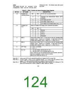
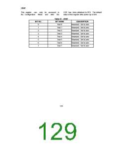
CR05
This register can only be accessed in the
Configuration Mode and the CSR has been
Table 52 - CR05- Floppy Disk and IDE Extended Setup Register
BIT NAME DESCRIPTION
Reserved Read Only. A read returns a 0.
BIT NO.
0,1
2
FDC DMA Mode 0=(default) Burst mode is enabled for the FDC FIFO execution
phase data transfers. 1=Non-Burst mode enabled. The FDRQ
and FIRQ pins are strobed once for each byte transferred while
the FIFO is enabled.
4,3
DenSel
Bit 4
Bit 3
Densel output
0
0
1
1
0
1
0
1
Normal (Default)
Reserved
1
0
5
6
7
Swap Drv 0,1
EXTx4
A high level on this bit, swaps drives and motor sel 0 and 1 of the
FDC. A low level on this bit does not (Default).
External 4 drive support: 0=Internal 2 drive decoder (default).
1=External 4 drive decoder (External 2 to 4 decoder required).
Reserved
Read Only. A read of this bit returns a 0
of this register after power up is FFH. This
CR06
This register can only be accessed in the
Configuration Mode and after the CSR has
been initialized to 06H. The default value
register holds the floppy disk drive types for up
to four floppy disk drives.
125

 SMSC [ SMSC CORPORATION ]