Legacy-Free Keyboard/Embedded Controller with SPI and LPC Docking Interface
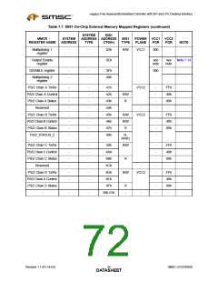
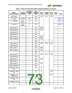
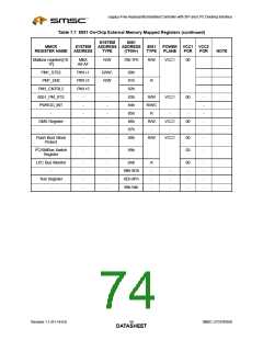
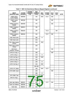
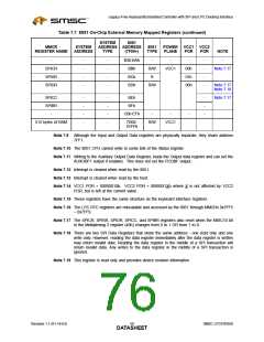
Table 7.7 8051 On-Chip External Memory Mapped Registers (continued)
SYSTEM
8051
MMCR
SYSTEM
ADDRESS ADDRESS
8051
POWER VCC1 VCC2
REGISTER NAME
ADDRESS
TYPE
(7F00+)
TYPE
PLANE
POR
POR
NOTE
-
-
-
-
-
-
-
-
-
B3h-BAh
BBh
-
-
-
-
-
-
-
-
SPICR
SPISR
SPIDR
R/W
R
VCC1
00h
01h
00h
Note 7.17
BCh
BDh
R/W
Note 7.17
Note 7.18
SPICC
-
-
-
-
-
-
-
-
BEh
BFh
-
-
-
Note 7.17
SPIBR
-
C0h-EFh
-
-
-
512 bytes of RAM
7D00-
R/W
VCC1
7EFFh
Note 7.9 Although the Input and Output Data registers are physically separate, they share address
7FF1.
Note 7.10 The 8051 CPU cannot write to some bits of the Status register.
Note 7.11 Writing to the Auxiliary Output Data Register, loads the Output data register and can set the
AUXOBF1 output if enabled. This does not set the PCOBF output.
Note 7.12 Interrupt is cleared when read by the 8051.
Note 7.13 Interrupt is cleared when read by the host.
Note 7.14 VCC1 POR = 00000X10b, VCC2 POR = 00000X1Xb where X is not affected by VCC2
POR, but is left at the current value.
Note 7.15 These registers have the same structure as the keyboard interface registers.
Note 7.16 The LPC RTC registers are relocatable and accessed by the 8051 through MMCRs 0x7FF5
– 0x7FF9.
Note 7.17 The SPICR, SPISR, SPIDR, SPICC, and SPIBR registers also reset when the MISC10 bit
in the Multiplexing 2 register (40h) changes from 0 to 1 OR from 1 to 0.
Note 7.18 There are two SPI Data Registers that share the same address - one read only and one
write only. However, reading the data register immediately after the data register is written
may return invalid data. Reading the data register in the middle of a SPI transaction will
return invalid data. Any writes to the data register in the middle of a SPI transaction is
ignored.
Note 7.19 This register is read only and provides device revision information.
Revision 1.1 (01-14-03)
SMSC LPC47N350
DATA5S8HEET

 SMSC [ SMSC CORPORATION ]