Legacy-Free Keyboard/Embedded Controller with SPI and LPC Docking Interface
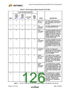
Note 9.2 The ATE PGM bit D2 in the Flash Program register is the PGM pin.
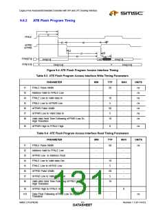
9.3
9.4
8051 Code Fetch Access
The 8051 Code Fetch Access function uses the 64k Embedded Flash as the 8051 program memory
space (). The 8051 Code Fetch Access function is enabled when bits D3 – D0 in the Flash Program
register are ‘0’ (see Table 9.1 and Section 9.10, "Flash Program Register").
Note: When the 8051 Code Fetch Access function is selected and the MMC bit is ‘1’, the 8051 can
execute from the 64k Embedded Flash and from the Scratch ROM (see Section 9.11, "Scratch
ROM").
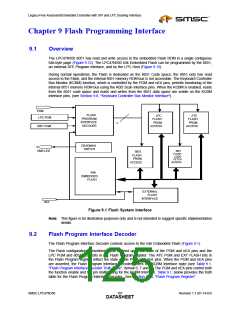
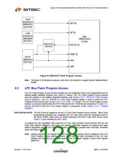
8051 Flash Program Access
The 8051 Flash Program Access function enables the 64k Embedded Flash to be programmed from an
internal parallel hardware interface using 8051 memory-mapped control registers (see Section 9.10.7,
"8051/LPC Flash Program Access Registers" and Figure 9.2). The 8051 PGM bit D0 in the Flash
Program register is used to enable the 8051 Program Access function (see Section 9.10.6, "8051 PGM
– D0").
APPLICATION NOTE: The 8051 must only execute program code from the 512-byte Scratch ROM to use the 8051
Flash Program Access function (see Section 9.11, "Scratch ROM"). When Flash
programming operations are completed, the 8051 must return the Embedded Flash to the
READ ARRAY state (Table 8.6) before returning to the 8051 Code Fetch Access mode
(Table 9.1). The 8051 must return the Embedded Flash to Read-Array mode when
programming has been completed before jumping out of the Scratch ROM code space.
To program the 64k Embedded Flash using the 8051 Flash Program Access function, first use the HIGH
ADDRESS (0x7FB0) and LOW ADDRESS (0x7FB1) registers for program and page address arguments
and then the DATA register (0x7FB2) for program data, read data, command codes and status data.
Note: Address arguments for Program Byte and Page Erase operations must be initialized in the 8051
Flash Program Access address registers before read and write commands to the CSI Host
Interface are activated by reads and writes to the 8051 Flash Program Access DATA register
(0x7FB2).
For information regarding the programming sequence for the LPC47N350 64k Embedded Flash, see
Section 8.3, "Command Sequence Interface (CSI)".
SMSC LPC47N350
109
Revision 1.1 (01-14-03)
DATASHEET

 SMSC [ SMSC CORPORATION ]