ST7781
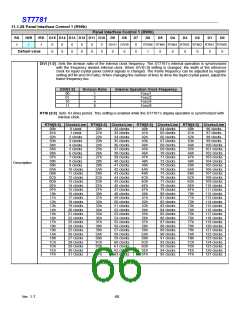
11.1.22 Horizontal and Vertical RAM Address Position (R50h, R51h, R52h, R53h)
Horizontal and Vertical RAM Address Position(R50h,R51h,R52h,R53h)
RS /WR /RD D15 D14 D13 D12 D11 D10 D9
D8
0
D7
D6
D5
D4
D3
D2
D1
D0
R50h
0
0
0
0
0
0
0
0
0
0
0
0
0
0
0
0
0
0
0
0
0
0
0
0
0
0
0
0
0
0
0
0
0
0
0
0
0
0
0
0
0
0
0
0
0
0
0
0
0
0
0
0
0
0
0
0
HSA7 HSA6 HSA5 HSA4 HSA3 HSA2 HSA1 HSA0
1
↑
1
1
1
1
0
0
0
0
Default value
0
0
0
0
0
0
HEA7 HEA6 HEA5 HEA4 HEA3 HEA2 HEA1 HEA0
R51h
Default value
R52h
Default value
R53h
Default value
1
↑
0
1
1
1
0
1
1
1
1
VSA8 VSA7 VSA6 VSA5 VSA4 VSA3 VSA2 VSA1 VSA0
1
↑
0
0
0
0
0
0
0
0
0
VEA8 VEA7 VEA6 VEA5 VEA4 VEA3 VEA2 VEA1 VEA0
1
↑
1
0
0
1
1
1
1
1
1
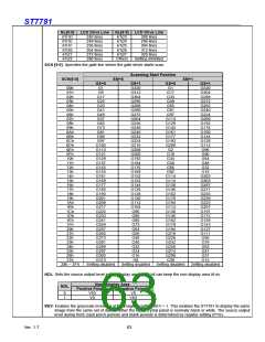
HSA [7:0], HEA [7:0] HSA[7:0] and HEA[7:0] are the start and end addresses of the window address area in
horizontal direction, respectively. HSA [7:0] and HEA [7:0] specify the horizontal range to write data. Set HSA [7:0]
and HEA [7:0] before starting RAM write operation. In setting, make sure that 8’h00 ≤ HAS < HEA ≤ 8’hEF
VSA [8:0], VEA [8:0] VSA [8:0] and VEA [8:0] are the start and end addresses of the window address area in
vertical direction, respectively. VSA [8:0] and VEA [8:0] specify the vertical range to write data. Set VSA [8:0] and
VEA [8:0] before starting RAM write operation. In setting, make sure that 9’h000 ≤ VSA < VEA ≤ 9’h13F.
Description
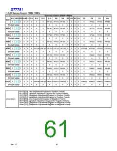
11.1.23 Gate Scan Control (R60h, R61h)
Gate Scan Control (R60h,R61h)
RS /WR /RD D15 D14 D13 D12 D11 D10 D9
D8
NL0
0
D7
0
0
D6
0
0
0
0
D5
D4
D3
D2
D1
D0
R60h
GS
0
0
0
0
NL5
NL4
NL3
NL2
NL1
SCN5 SCN4 SCN3 SCN2 SCN1 SCN0
1
↑
1
0
0
0
0
0
0
0
0
0
0
0
0
0
0
0
0
NDL
0
0
0
0
0
REV
0
Default value
0
0
0
0
0
0
0
0
0
0
0
0
0
0
0
0
R61h
Default value
1
↑
1
GS: Sets the direction of scan by the gate driver. Set GS bit in combination with SM and SS bits for the convenience
of the display module configuration and the display direction.
When GS=0, the scan direction is from G1 to G320
When GS=1, the scan direction is from G320 to G1
NL [5:0]: Sets the number of lines to drive the LCD at an interval of 8 lines. The DRAM address mapping is not
affected by the number of lines set by NL[5:0]. The number of lines must be the same or more than the number of
lines necessary for the size of the liquid crystal panel.
Description
Ver. 1.7
62

 SITRONIX [ SITRONIX TECHNOLOGY CO., LTD. ]