ST7781
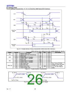
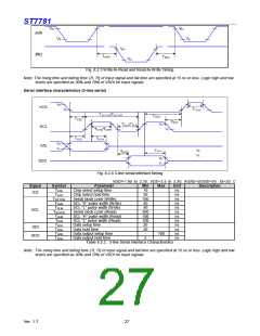
Fig. 8.2.3 Write-to-Read and Read-to-Write Timing
Note: The rising time and falling time (Tr, Tf) of input signal and fall time are specified at 15 ns or less. Logic high and low
levels are specified as 30% and 70% of VDDI for Input signals.
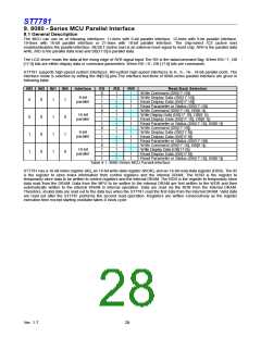
Serial interface characteristics (3-line serial)
Fig. 8.2.4 3-line serial interface timing
VDDI=1.65 to 3.3V, VDD=2.5 to 3.3V, AGND=DGND=0V, Ta=25
℃
Signal
Symbol
TCSS
TSCC
TSCYCW
TSHW
TSLW
TSCYCR
TSHR
TSLR
TSDS
TSDH
TSOD
Parameter
Chip select setup time
Chip select hold time
Serial clock cycle (Write)
SCL “H” pulse width (Write)
SCL “L” pulse width (Write)
Serial clock cycle (Read)
SCL “H” pulse width (Read)
SCL “L” pulse width (Read)
Data setup time
Min
10
50
100
40
40
200
100
100
20
20
-
Max
Unit
ns
ns
ns
ns
ns
ns
ns
ns
ns
ns
ns
ns
Description
/CS
SCL
SDI
Data hold time
Data output setup time
Data output hold time
100
-
SDO
TSOH
5
Table 8.2.2.: 3-line Serial Interface Characteristics
Note : The rising time and falling time (Tr, Tf) of input signal and fall time are specified at 15 ns or less. Logic high and low
levels are specified as 30% and 70% of VDDI for Input signals.
Ver. 1.7
27

 SITRONIX [ SITRONIX TECHNOLOGY CO., LTD. ]