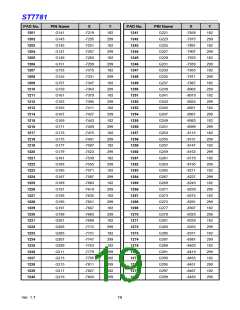
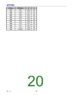
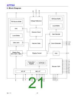
ST7781
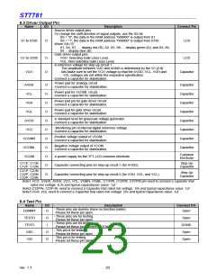
6.3 Driver Output Pin
Name
I/O
Description
Connect Pin
-Source driver output pins
-To change the shift direction of signal outputs, use the SS bit.
SS = “0”, the data in the RAM address “h00000” is output from S1.
SS = “1”, the data in the RAM address “h00000” is output from S720.
-When SS=”0”
S1 to S720
O
LCD
S1, S4, S7, … display red (R), S2, S5, S8, ... display green (G), and S3, S6,
S9 ... display blue (B)
-Gate driver output pins.
G1 to G320
VCI1
O
O
VGH: Selecting Gate Lines Level.
VGL: Non-selecting Gate Lines Level.
-A reference voltage for step-up circuit 1.
The amplitude between VDD and AGND is determined by the VC [2:0]
bits.Make sure to set the VCI1 voltage so that the AVDD, VCL, VGH and
VGL voltages are set within the respective specification.
-Connect a capacitor for stabilization.
LCD
Capacitor
-Power pad for analogy circuit.
AVDD
VCL
O
O
O
O
O
O
O
O
O
O
Capacitor
Capacitor
Capacitor
Capacitor
Capacitor
Capacitor
Capacitor
Capacitor
-
Connect a capacitor for stabilization.
-Power pad for VCOML circuit.
-Connect a capacitor for stabilization.
-Power pad pin for gate driver circuit.
-Connect a capacitor for stabilization.
VGH
-Power pad for gate driver circuit.
-Connect a capacitor for stabilization.
VGL
-A standard level for grayscale voltage generator.
-Connect a capacitor for stabilization.
GVDD
VCC
- Monitoring pin of internal digital reference voltage.
-Connect a capacitor for stabilization.
-Positive voltage output of VCOM.
-Connect a capacitor for stabilization.
VCOMH
VCOML
VCOM
-Negative voltage output of VCOM.
-Connect a capacitor for stabilization.
Common
Electrode
-A power supply for the TFT-LCD common electrode.
C11P, C11N
C12P, C12N
Step-Up
Capacitor
-Capacitor connecting pins for step-up circuit 1 (for AVDD).
C21P, C21N
C22P, C22N
C23P, C23N
Step-Up
Capacitor
O
-Capacitor connecting pins for step-up circuit 2 (for VGH, VGL, and VCL).
Note1.VCI1, GVDD, AVDD, VCC, VCL, VOMH, VOML, C11P/N, C12P/N, C21P/N pin need to connect a capacitor that
rated min voltage: 6.3v and typical capacitance value: 1uf
Note2.C22P/N, C23P /N, need to connect a Capacitor that rated min voltage: 10v and typical capacitance value: 1uf
Note3.VGH, VGL need to connect a Capacitor that rated min voltage: 25v and typical capacitance value: 1uf
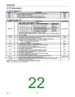
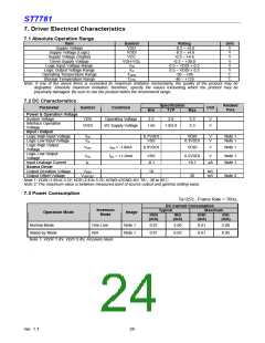
6.4 Test Pin
Name
I/O
Description
-These pins are dummy (have no function inside).
-Please let these pin open.
Connect Pin
DUMMY
O
Open
-These pins are for testing.
-Please let these pin open.
-These pins are for testing.
-Please let these pin connect to DGND.
-This pin is for testing.
-Please let these pin open.
-This pin is for testing.
-Please let these pin open.
TESTO
TESTI
OSC
O
I
Open
DGND
Open
Open
O
O
V25
Ver. 1.7
23

 SITRONIX [ SITRONIX TECHNOLOGY CO., LTD. ]