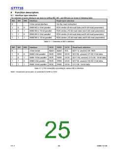
ST7735
9.3 Serial interface
The selection of this interface is done by IM2. See the Table 9.3.1.
IM2
0
SPI4W Interface
Read back selection
0
1
3-line serial interface
4-line serial interface
Via the read instruction (8-bit, 24-bit and 32-bit read parameter)
Via the read instruction (8-bit, 24-bit and 32-bit read parameter)
0
Table 9.3.1 Selection of serial interface
The serial interface is either 3-line/9-bit or 4-line/8-bit bi-directional interface for communication between the micro
controller and the LCD driver. The 3-line serial interface use: CSX (chip enable), SCL (serial clock) and SDA (serial data
input/output), and the 4-line serial interface use: CSX (chip enable), D/CX (data/ command flag), SCL (serial clock) and
SDA (serial data input/output). Serial clock (SCL) is used for interface with MCU only, so it can be stopped when no
communication is necessary.
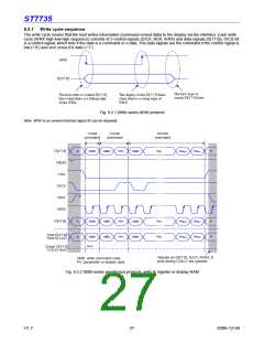
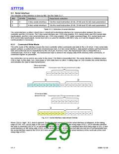
9.3.1 Command Write Mode
The write mode of the interface means the micro controller writes commands and data to the LCD driver. 3-line serial data
packet contains a control bit D/CX and a transmission byte. In 4-line serial interface, data packet contains just transmission
byte and control bit D/CX is transferred by the D/CX pin. If D/CX is “low”, the transmission byte is interpreted as a
command byte. If D/CX is “high”, the transmission byte is stored in the display data RAM (memory write command), or
command register as parameter.
Any instruction can be sent in any order to the driver. The MSB is transmitted first. The serial interface is initialized when
CSX is high. In this state, SCL clock pulse or SDA data have no effect. A falling edge on CSX enables the serial interface
and indicates the start of data transmission.
Fig. 9.3.1 Serial interface data stream format
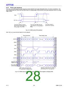
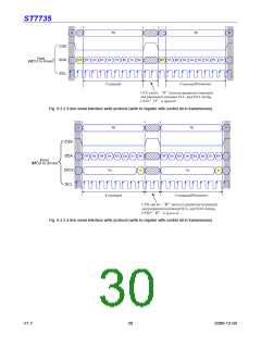
When CSX is “high”, SCL clock is ignored. During the high period of CSX the serial interface is initialized. At the falling
edge of CSX, SCL can be high or low (see Fig 9.3.2). SDA is sampled at the rising edge of SCL. D/CX indicates whether
the byte is command (D/CX=’0’) or parameter/RAM data (D/CX=’1’). D/CX is sampled when first rising edge of SCL (3-line
serial interface) or 8th rising edge of SCL (4-line serial interface). If CSX stays low after the last bit of command/data byte,
the serial interface expects the D/CX bit (3-line serial interface) or D7 (4-line serial interface) of the next byte at the next
rising edge of SCL.
V1.7
29
2009-12-04

 SITRONIX [ SITRONIX TECHNOLOGY CO., LTD. ]