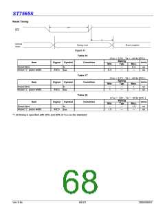
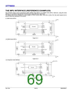
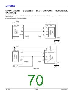
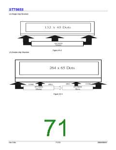
ST7565S
Revisions
Version
Description
0.1
Preliminary.
update Pad Center Coordinates page 2,3,4,5
0.2
0.2a
0.2b
0.2c
0.2d
0.2e
0.2f
0.3
update ABSOLUTE MAXIMUM RATINGS and DC CHARACTERISTICS
update DC CHARACTERISTICS , Pad Arrangement
update AC CHARACTERISTICS (serial)
update PIN DESCRIPTIONS M/S
update ABSOLUTE MAXIMUM RATINGS and DC CHARACTERISTICS
update Master and Slave reference example.
update Pad Center Coordinates (1/65 , 1/49 , 1/33 , 1/55 , 1/53 Duty) page 3..17
update Pad Diagram page2 and v5 regulator voltage diagram(figure 9) page35
Logic power supply VDD – VSS = 1.8V to 3.3 V (+10% Range), VOUT= -13V (+10% Range)
Modify page-38 The temperature grade of the Internal Power Supply for ST7565S (-0.05%/°C) Figure 14
Delete recommended to connect an external resistor to stabilize potentials of V1, V2, V3 and V4
Modify Tdh (data hold time) and page53,54 initial flow
0.3a
0.3b
0.3c
0.4
0.5
Solve Font issue.
Fix Page 2 values.
0.6a
Redraw some figures.
Rewrite some description for easy understanding.
Fix Word problems.
0.6b
0.6c
Modify mistake if Status Read.
Add I/O Pin ITO Resister Limitation.
Modify the mistake of The Reset Circuit.
Ver 0.6c
72/72
2009/09/07

 SITRONIX [ SITRONIX TECHNOLOGY CO., LTD. ]