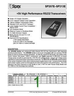
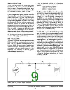
FEATURES
Charge–Pump
As in the original RS-232 multi-channel
products, the SP207E Series multi–channel
RS-232 line transceivers provide a variety of
configurations to fit most communication
needs,especiallythoseapplicationswhere+12V
isnotavailable. AllmodelsinthisSeriesfeature
low–power CMOS construction and SIPEX–
proprietary on-board charge pump circuitry to
generate the +10V RS-232 voltage levels. The
ability to use 0.1µF charge pump capacitors
saves board space and reduces circuit cost.
Different models within the Series provide
different driver/receiver combinations to
match any application requirement.
The charge pump is a Sipex–patented design
(5,306,954) and uses a unique approach
compared to older less–efficient designs. The
chargepumpstillrequiresfourexternalcapacitors,
but usesa four–phase voltage shiftingtechnique
to attain symmetrical 10V power supplies.
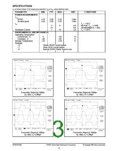
Figure 3a shows the waveform found on the
positive side of capcitor C , and Figure 3b
shows the negative side of ca2pcitor C2. There is
a free–running oscillator that controls the four
phases of the voltage shifting. A description of
each phase follows.
Phase 1
—VSS chargestorage—Duringthisphaseofthe
clock cycle, the positive side of capacitors C1
and C2 are initially charged to +5V. Cl+ is then
switched to ground and the charge in C1– is
The SP211 and SP213E models feature a low–
power shutdown mode, which reduces power
supply drain to 1µA. The SP213E includes a
Wake-Up function which keeps two receivers
active in the shutdown mode, unless disabled by
the EN pin.
–
transferred to C . Since C + is connected to
+5V, the voltage2potential ac2ross capacitor C2 is
now 10V.
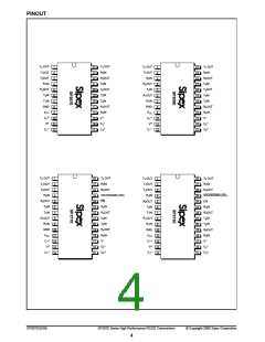
The family is available in 28–pin SO (wide) and
SSOP (shrink) small outline packages. Devices
can be specified for commercial (0°C to +70°C)
and industrial/extended (–40°C to +85°C)
operating temperatures.
Phase 2
— VSS transfer — Phase two of the clock
connects the negative terminal of C to the VSS
storage capacitor and the positive ter2minal of C2
to ground, and transfers the generated –l0V to
C3. Simultaneously, the positive side of
capacitorC1 isswitchedto+5Vandthenegative
side is connected to ground.
THEORY OF OPERATION
The SP207E Series devices are made up of
three basic circuit blocks — 1) transmitter/
driver, 2) receiver and 3) the SIPEX–
proprietary charge pump. Each model within
the Series incorporates variations of these
circuits to achieve the desired configuration
and performance.
Phase 3
— VDD charge storage — The third phase of the
clock is identical to the first phase — the charge
transferred in C1 produces –5V in the negative
terminal of C1, which is applied to the negative
side of capacitor C . Since C2+ is at +5V, the
voltage potential acr2oss C2 is l0V.
V
= +5V
CC
C
4
+5V
+
–
+
V
V
Storage Capacitor
Storage Capacitor
DD
SS
+
–
+
–
C
C
2
1
–
C
–5V
–5V
3
Figure 1. Charge Pump — Phase 1
SP207EDS/09
SP207E Series High Performance Transceivers
© Copyright 2000 Sipex Corporation
5

 SIPEX [ SIPEX CORPORATION ]