Power Dissipation Per Package
ABSOLUTE MAXIMUM RATINGS
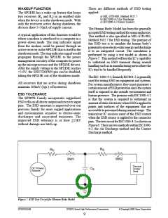
These are stress ratings only and functional
operation of the device at these or any other
above those indicated in the operation sections
of the specifications below is not implied. Exposure
to absolute maximum rating conditions for extended
periods of time may affect reliability.
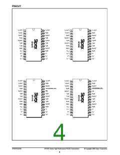
24-pin SSOP (derate 11.2mW/oC above +70oC)....900mW
24-pin PDIP (derate 15.9mW/oC above +70oC)....1300mW
24-pin SOIC (derate 12.5mW/oC above +70oC)...1000mW
28-pin SSOP (derate 11.2mW/oC above +70oC)....900mW
28-pin SOIC (derate 12.7mW/oC above +70oC)...1000mW
VCC .................................................................. +6V
V+ ....................................... (VCC – 0.3V) to +13.2V
V– ................................................................ 13.2V
Input Voltages
TIN ..........................................–0.3V to (VCC +0.3V)
RIN ................................................................ ±20V
Output Voltages
TOUT ................................ (V+, +0.3V) to (V–, –0.3V)
ROUT ....................................... –0.3V to (VCC +0.3V)
Short Circuit Duration on TOUT .............. Continuous
.
SPECIFICATIONS
VCC at nominal ratings; 0.1µF charge pump capacitors; TMIN to TMAX, unless otherwise noted.
PARAMETER
MIN.
TYP.
MAX.
UNIT
CONDITIONS
TIN, EN, SD
TTL INPUTS
Logic Threshold
VIL
VIH
0.8
Volts
Volts
µA
2.0
Logic Pullup Current
Maximum Transmssion Rate
15
230
200
TIN = 0V
CL = 1000pF, RL = 3KΩ
120
kbps
TTL OUTPUTS
Compatibility
VOL
TTL/CMOS
0.05
0.4
Volts
Volts
µA
IOUT = 3.2mA; VCC = +5V
IOUT = –1.0mA
0V ≤ ROUT ≤ VCC ; SP211 EN = 0V;
VOH
3.5
Leakage Current
+10
SP213 EN = VCC
TA = +25°C
RS232 OUTPUT
Output Voltage Swing
+5
+7
Volts
All transmitter outputs loaded
with 3KΩ to ground
Output Resistance
300
Ω
VCC = 0V; VOUT = +2V
Output Short Circuit Current
+25
mA
Infinite duration, VOUT = 0V
RS232 INPUT
Voltage Range
Voltage Threshold
Low
High
Hysteresis
Resistance
–15
0.8
+15
Volts
1.2
1.7
0.5
5
Volts
Volts
Volts
kΩ
VCC = 5V, TA = +25°C
VCC = 5V, TA = +25°C
VCC = +5V
2.8
1.0
7
0.2
3
VIN =+15V; TA = +25°C
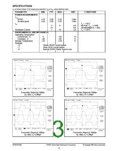
DYNAMIC CHARACTERISTICS
Driver Propagation Delay
Receiver Propagation Delay
Instantaneous Slew Rate
1.5
0.5
µs
µs
V/µs
TTL–to–RS-232
RS-232–to–TTL
1.5
30
CL = 50pF, RL = 3–7KΩ;
TA = +25°C; from +3V
CL = 2,500pF, RL = 3KΩ;
measured from +3V to –3V
or –3V to +3V
Transition Time
1.5
µs
Output Enable Time
Output Disable Time
400
250
ns
ns
SP207EDS/09
SP207E Series High Performance RS232 Transceivers
© Copyright 2000 Sipex Corporation
2

 SIPEX [ SIPEX CORPORATION ]