computer to power up the microprocessor and
the SP2XXB/SP213 drivers. After the supply
voltage to the SP2XXB/SP213 reaches +5.0V,
the SHUTDOWN pin can be disabled, taking
the SP2XXB/SP213 out of the shutdown mode.
A typical application of this function would be
where a modem is interfaced to a computer in a
power–down mode. The ring indicator signal
from the modem could be passed through an
active receiver in the SP2XXB/SP213 that is
itself in the shutdown mode. The ring indicator
signal would propagate through the SP2XXB/
SP213tothepowermanagementcircuitryofthe
All receivers that are active during shutdown
maintain 500mV (typ.) of hysteresis.
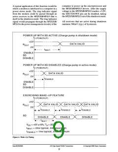
POWER UP WITH SD ACTIVE (Charge pump in shutdown mode)
t
0 (POWERUP)
+5V
DATA VALID
R
OUT
0V
t
WAIT
ENABLE
SD
DISABLE
POWER UP WITH SD DISABLED (Charge pump in active mode)
t
0 (POWERUP)
+5V
DATA VALID
R
OUT
0V
t
ENABLE
ENABLE
SD
DISABLE
EXERCISING WAKE–UP FEATURE
t
0 (POWERUP)
+5V
DATA VALID
DATA VALID
DATA VALID
R
OUT
0V
t
t
t
ENABLE
ENABLE
ENABLE
SD
DISABLE
ENABLE
DISABLE
t
WAIT
V
= +5V ±10%; T = 25°C
A
CC
t
t
= 2ms typical, 3ms maximum
WAIT
ENABLE
= 1ms typical, 2ms maximum
Figure 6. Wake–Up Timing
Date:05/26/2005
+5V High-Speed RS232 Transceivers
© Copyright 2005 Sipex Corporation
9

 SIPEX [ SIPEX CORPORATION ]