+10V
a) C2+
GND
GND
b) C2–
–10V
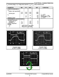
Figure 3. Charge Pump Waveforms
pump. Each model within the Series incorpo-
rates variations of these circuits to achieve the
desired configuration and performance.
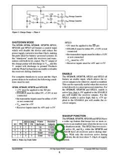
driver be left open, an internal 400kOhm pullup
resistor to VCC forces the input high, thus commit-
ting the output to a low state. The slew rate of the
transmitter output is internally limited to a maxi-
mumof30V/µsinordertomeettheEIAstandards
(EIA RS-232D 2.1.7, Paragraph 5). The transition
of the loaded output from high to low also meets
the monotonicity requirements of the standard.
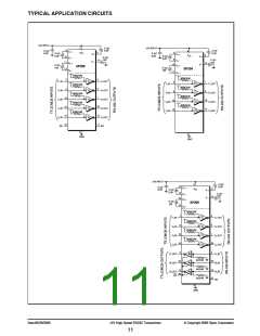
Transmitter/Driver
The drivers are inverting transmitters, which ac-
cept either TTL or CMOS inputs and output the
RS-232 signals with an inverted sense relative to
the input logic levels. Typically, the RS-232 out-
put voltage swing is ±9V with no load, and ±5V
minimum with full load. The transmitter outputs
are protected against infinite short–circuits to
ground without degradation in reliability. The
drivers of the SP200, SP206, SP206B, SP207B,
SP211, SP211B and SP213 can be tri–stated by
Receivers
The receivers convert RS-232 input signals to
inverted TTL signals. Since the input is usually
fromatransmissionlinewherelongcablelengths
and system interference can degrade the signal,
the inputs have a typical hysteresis margin of
500mV. This ensures that the receiver is virtu-
ally immune to noisy transmission lines. Should
aninputbeleftunconnected,a5kOhmpulldown
resistor to ground will commit the output of the
receiver to a high state.
using
the
SHUTDOWN
function.
Inthe“poweroff”state, theoutputimpedancewill
remaingreaterthan300Ohms,againsatisfyingthe
RS-232 specifications. Should the input of the
V
= +5V
CC
C
4
+5V
+
–
+
V
V
Storage Capacitor
Storage Capacitor
DD
+
–
+
–
C
C
2
1
–
SS
C
–5V
–5V
3
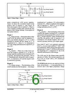
Figure 4. Charge Pump — Phase 3
Date:05/26/2005
+5V High-Speed RS232 Transceivers
© Copyright 2005 Sipex Corporation
7

 SIPEX [ SIPEX CORPORATION ]