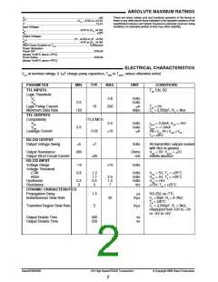
V
= +5V
CC
C
+5V
4
+
–
+
V
V
Storage Capacitor
Storage Capacitor
DD
+
–
+
–
C
C
2
1
–
SS
C
–5V
–5V
3
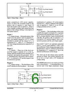
Figure 1. Charge Pump — Phase 1
attain symmetrical ±10V power supplies.
transferred in C1 produces –5V in the negative
terminal of C1, which is applied to the negative
side of capacitor C . Since C2+ is at +5V, the
voltage potential ac2ross C2 is l0V.
Figure 3a shows the waveform found on the
positive side of capcitor C , and Figure 3b
shows the negative side of ca2pcitor C2. There is
a free–running oscillator that controls the four
phases of the voltage shifting. A description of
each phase follows.
Phase 4
— V transfer — The fourth phase of the clock
connDeDcts the negative terminal of C2 to ground,
and transfers the generated l0V across C2 to C ,
theV storagecapacitor.Again,simultaneousl4y
with DthDis, the positive side of capacitor C is
switched to +5V and the negative side is c1on-
nected to ground, and the cycle begins again.
Phase 1
—VSS chargestorage—Duringthisphaseofthe
clock cycle, the positive side of capacitors C1
and C2 are initially charged to +5V. Cl+ is then
switched to ground and the charge in C1– is
transferred to C –. Since C + is connected to
+5V, the voltage2potential ac2ross capacitor C2 is
now 10V.
Since both V+ and V– are separately generated
from VCC; in a no–load condition V+ and V– will
be symmetrical. Older charge pump approaches
that generate V– from V+ will show a decrease in
the magnitude of V– compared to V+ due to the
inherent inefficiencies in the design.
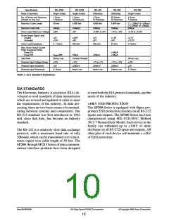
Phase 2
— V transfer — Phase two of the clock con-
nectsSSthe negative terminal of C2 to the VSS
storage capacitor and the positive terminal of C2
to ground, and transfers the generated –l0V to
C3. Simultaneously, the positive side of capaci-
tor C 1 is switched to +5V and the negative side
is connected to ground.
The clock rate for the charge pump typically
operates at 15kHz. The external capacitors can
be as low as 0.1µF with a 16V breakdown
voltage rating.
The SP200 Series devices are made up of three
basic circuit blocks — 1) transmitter/driver, 2)
receiver and 3) the Sipex proprietary charge
Phase 3
— VDD charge storage — The third phase of the
clock is identical to the first phase — the charge
V
= +5V
CC
C
4
+
–
+
V
V
Storage Capacitor
Storage Capacitor
DD
+
–
+
–
C
C
2
1
–
SS
C
–10V
3
Figure 2. Charge Pump — Phase 2
Date:05/26/2005
+5V High-Speed RS232 Transceivers
© Copyright 2005 Sipex Corporation
6

 SIPEX [ SIPEX CORPORATION ]