SiI 1160 PanelLink Transmitter
Data Sheet
LIST OF TABLES
Table 1. General I2C Register Bits................................................................................................................ 13
Table 2. Dual Zone PLL I2C Control Register Bits........................................................................................ 14
Table 3. One Pixel/Clock Input/Output TFT Mode........................................................................................ 15
Table 4. Two Pixels/Clock Input/Output TFT Mode ...................................................................................... 16
Table 5. 24-bit One Pixel/Clock Input with 24-bit Two Pixels/Clock Output TFT Mode................................ 17
Table 6. 18-bit One Pixel/Clock Input with 18-bit Two Pixels/Clock Output TFT Mode................................ 18
Table 7. Two Pixels/Clock Input with One Pixel/Clock Output TFT Mode.................................................... 19
Table 8. New Pin Functions for SiI 1160 Tx.................................................................................................. 20
Table 9. Power Consumption Characteristics .............................................................................................. 22
Table 10. Recommended Components for Bypass and Decoupling Circuits............................................... 23
Table 11. Routing Guidelines for DVI Traces................................................................................................ 27
LIST OF FIGURES
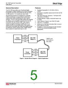
Figure 1. System Block Diagram – Typical Application.................................................................................. 1
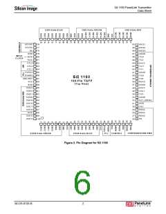
Figure 2. Pin Diagram for SiI 1160 ................................................................................................................. 2
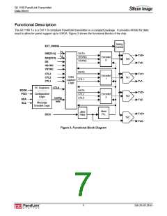
Figure 3. Functional Block Diagram ............................................................................................................... 3
Figure 4. Clock Cycle High/Low Times........................................................................................................... 6
Figure 5. Input Data Setup/Hold Time to IDCK .............................................................................................. 6
Figure 6. VSYNC, HSYNC and CTL[3:1] Delay Time from DE...................................................................... 6
Figure 7. DE High and Low Times.................................................................................................................. 6
Figure 8. Reset Timing at Power-Up or Prior to First I2C Access................................................................... 7
Figure 9. I2C Byte Read................................................................................................................................ 11
Figure 10. I2C Byte Write.............................................................................................................................. 11
Figure 11. Voltage Regulation using LM317EMP......................................................................................... 20
Figure 12. Planned Spread Spectrum Support Circuit ................................................................................. 21
Figure 13. Typical Reset Circuit.................................................................................................................... 22
Figure 14. Decoupling and Bypass Capacitor Placement............................................................................ 23
Figure 15. Decoupling and Bypass Schematic............................................................................................. 23
Figure 16. Series Input Damping Resistors for Driving Source ................................................................... 24
Figure 17. Differential Output Source Terminations .................................................................................... 24
Figure 18. Source Termination Layout Illustration........................................................................................ 25
Figure 19. Example of Incorrect Differential Signal Routing ........................................................................ 26
Figure 20. Example of Correct Differential Signal Routing........................................................................... 26
Figure 21. Differential Trace Routing to DVI Connector (Top Side View) .................................................... 26
Figure 22. 100-pin TQFP Package Dimensions (JEDEC code MS-026-AED) ............................................ 28
SiI-DS-0126-B
iv

 SILICONIMAGE [ Silicon image ]