SC9821C
(Continued)
Symbol
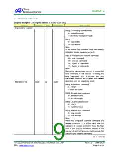
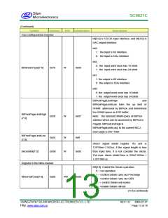
Esp configuration register
Address
R/W
Initialization
Description
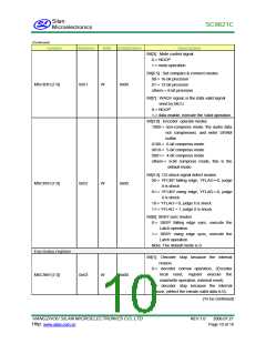
bit[3:2] is CD•DA input interface, and bit[1:0] is
DAC output interface.
bit3:
1: the input is IIS interface
0: the input is EIAJ interface
bit2:
0: the input word clock has 16 bitclk
1: the input word clock has 24 bitclk
BitStreamType[7:0]
0x76
W
0x00
bit1:
1: the output is IIS interface
0: the output is EIAJ interface
bit0:
0: the output word clock has 16 bitclk
1: the output word clock has 24 bitclk
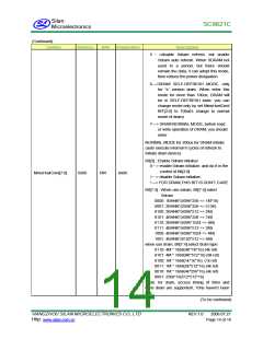
BitPoolPageLimitHigh
an
BitPoolPageLimitLow
form
the
up
limit
of
DRAM addressed by BitPool, and determined
the DRAM space as ESP buffer;
BitPoolPageLimitHigh
[7:0]
0x58
W
0x07
Note: the external DRAM space of BitPool
address which can be accessed by BitPool is
Page[0, BitPoolLimitHigh &
BitPoolPageLimitLow]. In the current MCU,
each page is 256×16bit
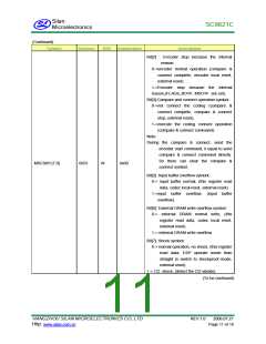
BitPoolPageLimitLow
[7:0]
0x59
0x5B
W
W
0xff
Shock
signal
shield
register.
It’s
unit
is
128*59ns=7.552us, if the signal length is less
than input time, it is not consider the shock.
The max. shock shield time is 255x7.552us =
1,925.880 us.
ShockMsk[7:0]
0x00
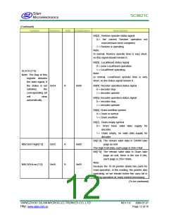
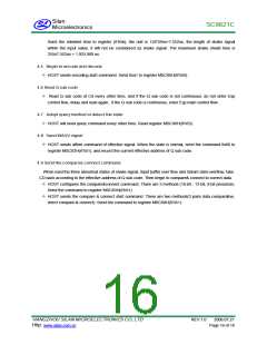
Register in the Mmu module
Bit[2:0]: Control the Sdram operation:
0ˉ>no operation
1ˉ>control Sdram carry out Precharge
2ˉ>control Sdram carry out CBR
3ˉ> control Sdram set modes
4ˉ>enable Sdram refresh
MmuHostCmd[7:0]
0x00
RW
0x08
(To be continued)
HANGZHOU SILAN MICROELECTRONICS CO.,LTD
Http:
REV:1.0
2006.07.21
www.silan.com.cn
Page 13 of 18

 SILAN [ SILAN MICROELECTRONICS JOINT-STOCK ]