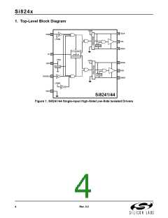
Si824x
Table 2. Absolute Maximum Ratings1
Parameter
Symbol
Min
–65
–40
–0.6
–0.6
–0.5
—
Typ
—
—
—
—
—
—
—
—
—
—
Max
+150
+125
6.0
Units
°C
2
Storage Temperature
T
STG
Ambient Temperature under Bias
Input-side Supply Voltage
T
°C
A
VDDI
VDDA, VDDB
VIN
V
Driver-side Supply Voltage
30
V
Voltage on any Pin with respect to Ground
Output Drive Current per Channel
Lead Solder Temperature (10 sec)
VDD + 0.5
10
V
I
mA
°C
O
—
260
3
Latchup Immunity
—
100
V/ns
Maximum Isolation (Input to Output)
Maximum Isolation (Output to Output)
Notes:
—
2500
1500
V
V
RMS
RMS
—
1. Permanent device damage may occur if the absolute maximum ratings are exceeded. Functional operation should be
restricted to the conditions as specified in the operational sections of this data sheet. Exposure to absolute maximum
rating conditions for extended periods may affect device reliability.
2. VDE certifies storage temperature from –40 to 150 °C.
3. Latchup immunity specification is for slew rate applied across GNDI and GNDA or GNDB.
Table 3. Regulatory Information*
CSA
The Si824x is certified under CSA Component Acceptance Notice 5A. For more details, see File 232873.
61010-1: Up to 300 V
60950-1: Up to 300 V
VDE
reinforced insulation working voltage; up to 600 V
reinforced insulation working voltage; up to 600 V
basic insulation working voltage.
basic insulation working voltage.
RMS
RMS
RMS
RMS
The Si824x is certified according to IEC 60747-5-2. For more details, see File 5006301-4880-0001.
60747-5-2: Up to 560 V
for basic insulation working voltage.
peak
UL
The Si824x is certified under UL1577 component recognition program. For more details, see File E257455.
Rated up to 2500 V isolation voltage for basic protection.
RMS
*Note: Regulatory Certifications apply to 2.5 kVRMS rated devices, which are production tested to 3.0 kVRMS for 1 sec.
For more information, see "6.Ordering Guide" on page 25.
8
Rev. 0.2

 SILICON [ SILICON ]