Si824x
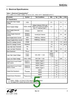
Table 1. Electrical Characteristics1 (Continued)
4.5 V < VDDI < 5.5 V, VDDA = VDDB = 12 V or 15 V. TA = –40 to +125 °C. Typical specs at 25 °C
Parameter
Symbol
VDDIUV+
VDDIUV–
VDDIHYS
VDDAUV+
Test Conditions
VDDI rising
Min
3.60
3.30
—
Typ
4.0
Max
4.45
4.15
—
Units
V
VDDI Undervoltage Threshold
VDDI Undervoltage Threshold
VDDI Lockout Hysteresis
VDDI falling
3.70
250
V
mV
,
VDDA, VDDB Undervoltage
Threshold
VDDA, VDDB rising
VDDBUV+
See Figure 34 on page 21.
See Figure 35 on page 21.
7.50
9.60
8.60
11.1
9.40
12.2
V
V
8 V Threshold
10 V Threshold
VDDAUV–
VDDBUV–
,
VDDA, VDDB Undervoltage
Threshold
VDDA, VDDB falling
See Figure 34 on page 21.
See Figure 35 on page 21.
7.20
9.40
8.10
10.1
8.70
10.9
V
V
8 V Threshold
10 V Threshold
VDDAHYS
VDDBHYS
,
VDDA, VDDB
Lockout Hysteresis
UVLO voltage = 8 V
UVLO voltage = 10 V
—
—
600
—
—
mV
mV
VDDAHYS
VDDBHYS
,
VDDA, VDDB
Lockout Hysteresis
1000
AC Specifications
Minimum Pulse Width
—
—
—
10
25
—
60
ns
ns
ns
tPHL, tPLH
PWD
CL = 1 nF
Propagation Delay
Pulse Width Distortion
1.0
5.60
|t
- t
|
PLH PHL
Programmed Dead Time2
DT
See Figures 36 and 37
CL = 1 nF (Si8241)
CL = 1 nF (Si8244)
0.4
—
—
—
—
1000
20
ns
ns
ns
tR,tF
Output Rise and Fall Time
—
12
Shutdown Time from
Disable True
tSD
—
—
—
25
—
—
5
60
60
7
ns
ns
µs
Restart Time from
Disable False
tRESTART
tSTART
CMTI
Time from VDD_ = VDD_UV+
to VOA, VOB = VIA, VIB
Device Start-up Time
Common Mode
Transient Immunity
VIA, VIB, PWM = VDDI or 0 V
45
—
kV/µs
Notes:
1. VDDA = VDDB = 12 V for 8 V UVLO and 10 V UVLO devices.
2. The largest RDT resistor that can be used is 220 k.
6
Rev. 0.2

 SILICON [ SILICON ]