Si824x
5. Pin Descriptions
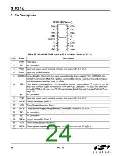
SOIC-16 (Narrow)
1
16
15
14
13
PWM
NC
VDDA
VOA
GNDA
NC
2
3
4
5
6
7
8
VDDI
GNDI
DISABLE
DT
Si8241/44
12
11
10
9
NC
VDDB
VOB
GNDB
NC
VDDI
Table 11. Si8241/44 PWM Input HS/LS Isolated Driver (SOIC-16)
Description
Pin
1
Name
PWM PWM input.
NC No connection.
2
3
VDDI Input-side power supply terminal; connect to a source of 4.5 to 5.5 V.
GNDI Input-side ground terminal.
4
5
DISABLE Device Disable. When high, this input unconditionally drives outputs VOA, VOB LOW. It is
strongly recommended that this input be connected to external logic level to avoid erroneous
operation due to capacitive noise coupling.
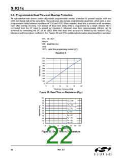
6
DT
Dead time programming input. The value of the resistor connected from DT to ground sets the
dead time between output transitions of VOA and VOB. Defaults to 1 ns dead time when con-
nected to VDDI or left open (see "3.8.Programmable Dead Time and Overlap Protection" on
page 22).
7
NC
No connection.
8
VDDI Input-side power supply terminal; connect to a source of 4.5 to 5.5 V.
GNDB Ground terminal for Driver B.
9
10
11
12
13
14
15
16
VOB Driver B output (low-side driver).
VDDB Driver B power supply voltage terminal; connect to a source of 6.5 to 24 V.
NC
NC
No connection.
No connection.
GNDA Ground terminal for Driver A.
VOA Driver A output (high-side driver).
VDDA Driver A power supply voltage terminal; connect to a source of 6.5 to 24 V.
24
Rev. 0.2

 SILICON [ SILICON ]