Si824x
4. Applications
The following examples illustrate typical circuit configurations using the Si824x.
4.1. Class D Digital Audio Driver
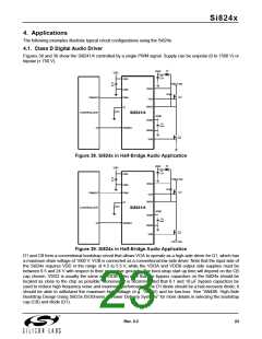
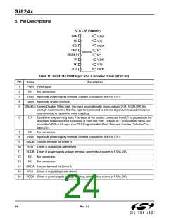
Figures 38 and 39 show the Si8241/4 controlled by a single PWM signal. Supply can be unipolar (0 to 1500 V) or
bipolar (± 750 V).
D1
VDD2
C2
VDDI
1 µF
VDDI
C1
1uF
1500 V max
VDDA
GNDI
PWM
CB
Q1
PWMOUT
CONTROLLER
I/O
VOA
GNDA
DT
RDT
Si8241/4
VDDB
VDDB
C3
10uF
DISABLE
GNDB
VOB
Q2
Figure 38. Si824x in Half-Bridge Audio Application
D1
VDD2
C2
VDDI
1 µF
VDDI
C1
1uF
+750 V max
VDDA
GNDI
PWM
CB
Q1
PWMOUT
CONTROLLER
I/O
VOA
GNDA
DT
RDT
Si8241/4
VDDB
VDDB
C3
10uF
DISABLE
GNDB
VOB
Q2
-750 V max
Figure 39. Si824x in Half-Bridge Audio Application
D1 and CB form a conventional bootstrap circuit that allows VOA to operate as a high-side driver for Q1, which has
a maximum drain voltage of 1500 V. VOB is connected as a conventional low-side driver. Note that the input side of
the Si824x requires VDD in the range of 4.5 to 5.5 V, while the VDDA and VDDB output side supplies must be
between 6.5 and 24 V with respect to their respective grounds. The boot-strap start up time will depend on the CB
cap chosen. VDD2 is usually the same as VDDB. Also note that the bypass capacitors on the Si824x should be
located as close to the chip as possible. Moreover, it is recommended that 0.1 and 10 µF bypass capacitors be
used to reduce high frequency noise and maximize performance. The D1 diode should be a fast-recovery diode; it
should be able to withstand the maximum high voltage (e.g. 1500 V) and be low-loss. See “AN486: High-Side
Bootstrap Design Using Si823x ISODrivers in Power Delivery Systems” for more details in selecting the bootstrap
cap (CB) and diode (D1).
Rev. 0.2
23

 SILICON [ SILICON ]