C8051F52x-53x
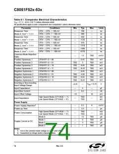
Table 8.1. Comparator Electrical Characteristics
VDD = 2.1 V, –40 to +125 °C unless otherwise noted.
All specifications apply to both Comparator0 and Comparator1 unless otherwise noted.
Parameter
Conditions
CP0+ – CP0– = 100 mV
CP0+ – CP0– = –100 mV
CP0+ – CP0– = 100 mV
CP0+ – CP0– = –100 mV
CP0+ – CP0– = 100 mV
CP0+ – CP0– = –100 mV
CP0+ – CP0– = 100 mV
CP0+ – CP0– = –100 mV
Min
—
—
—
—
—
—
—
—
Typ
780
Max
—
Units
ns
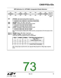
Response Time:
1
Mode 0, Vcm = 1.5 V
980
—
ns
850
—
ns
Response Time:
1
Mode 1, Vcm = 1.5 V
1120
870
—
ns
—
ns
Response Time:
1
Mode 2, Vcm = 1.5 V
1310
1980
4770
—
ns
—
ns
Response Time:
1
Mode 3, Vcm = 1.5 V
—
ns
Common-Mode Rejection
Ratio
—
1.5
TBD
mV/V
Positive Hysteresis 1
Positive Hysteresis 2
Positive Hysteresis 3
Positive Hysteresis 4
Negative Hysteresis 1
Negative Hysteresis 2
Negative Hysteresis 3
Negative Hysteresis 4
CP0HYP1-0 = 00
CP0HYP1-0 = 01
CP0HYP1-0 = 10
CP0HYP1-0 = 11
CP0HYN1-0 = 00
CP0HYN1-0 = 01
CP0HYN1-0 = 10
CP0HYN1-0 = 11
—
0.45
5
TBD
TBD
TBD
TBD
TBD
TBD
TBD
TBD
mV
mV
mV
mV
mV
mV
mV
mV
TBD
TBD
TBD
—
9.95
19.47
0.45
4.99
9.93
19.41
TBD
TBD
TBD
Inverting or Non-Inverting
Input Voltage Range
V
+ 0.25
–0.25
—
V
DD
Input Capacitance
Input Bias Current
Input Offset Voltage
—
—
4
—
—
10
pF
nA
0.5
—
–10
mV
High Speed Mode (CP1HIQE = ‘1’)
Low Speed Mode (CP1HIQE = ‘0’)
TBD
TBD
kΩ
kΩ
Input Impedance
—
—
Power Supply
2
—
—
0.2
2.3
4
mV/V
µs
Power Supply Rejection
Power-up Time
—
High Speed Mode (CP1HIQE = ‘1’)
Low Speed Mode (CP1HIQE = ‘0’)
TBD
TBD
mA
mA
Power Consumption
—
—
Mode 0
Mode 1
Mode 2
Mode 3
—
—
—
—
13
6
TBD
TBD
TBD
TBD
µA
µA
µA
µA
Supply Current at DC
3
1
Notes:
1. Vcm is the common-mode voltage on CP0+ and CP0–.
2. Guaranteed by design and/or characterization.
74
Rev. 0.3

 SILICON [ SILICON ]