C8051F52x-53x
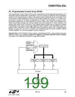
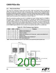
20.1. PCA Counter/Timer
The 16-bit PCA counter/timer consists of two 8-bit SFRs: PCA0L and PCA0H. PCA0H is the high byte
(MSB) of the 16-bit counter/timer and PCA0L is the low byte (LSB). Reading PCA0L automatically latches
the value of PCA0H into a “snapshot” register; the following PCA0H read accesses this “snapshot” register.
Reading the PCA0L Register first guarantees an accurate reading of the entire 16-bit PCA0 counter.
Reading PCA0H or PCA0L does not disturb the counter operation. The CPS2-CPS0 bits in the PCA0MD
register select the timebase for the counter/timer as shown in Table 20.1.
When the counter/timer overflows from 0xFFFF to 0x0000, the Counter Overflow Flag (CF) in PCA0MD is
set to logic 1 and an interrupt request is generated if CF interrupts are enabled. Setting the ECF bit in
PCA0MD to logic 1 enables the CF flag to generate an interrupt request. The CF bit is not automatically
cleared by hardware when the CPU vectors to the interrupt service routine, and must be cleared by soft-
ware (Note: PCA0 interrupts must be globally enabled before CF interrupts are recognized. PCA0 interrupts
are globally enabled by setting the EA bit (IE.7) and the EPCA0 bit in EIE1 to logic 1). Clearing the CIDL bit
in the PCA0MD register allows the PCA to continue normal operation while the CPU is in Idle mode.
Table 20.1. PCA Timebase Input Options
CPS2
CPS1
CPS0
Timebase
0
0
0
0
1
1
1
0
0
1
1
0
0
1
0
1
0
1
0
1
0
System clock divided by 12
System clock divided by 4
Timer 0 overflow
High-to-low transitions on ECI (max rate = system clock divided by 4)
System clock
External oscillator source divided by 8*
RTC clock divided by 8*
*Note: External clock divided by 8 and RTC0 clock divided by 8 are synchronized with the system clock.
IDLE
PCA0MD
C W W C C C E
D D P P P C
PCA0CN
C C C
C C
F R
I
C C C
F F F
2 1 0
D T
L E C
L
S S S F
2 1 0
To SFR Bus
PCA0L
read
K
Snapshot
Register
SYSCLK/12
SYSCLK/4
000
001
010
Timer 0 Overflow
ECI
0
Overflow
To PCA Interrupt System
PCA0H
PCA0L
1
011
100
101
CF
SYSCLK
To PCA Modules
External Clock/8
Figure 20.2. PCA Counter/Timer Block Diagram
200
Rev. 0.3

 SILICON [ SILICON ]