C8051F39x/37x
17.1. Program Memory
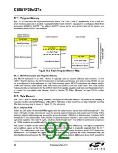
The CIP-51 core has a 64 kB program memory space. The C8051F39x/37x implements 16 kB of this pro-
gram memory space as in-system, re-programmable Flash memory, organized in a contiguous block from
addresses 0x0000 to 0x3FFF. The address 0x3FFF serves as the security lock byte for the device, and
addresses above 0x3FFF are reserved.
C8051F390/1/2/3
C8051F370/1/4/5
C8051F392/3/6/7
C8051F398/9
0x3FFF
0x3FFE
Lock Byte
Lock Byte Page
0x3E00
0x1FFF
0x1FFE
Lock Byte
Lock Byte Page
0x1E00
0x0FFF
0x0FFE
Lock Byte
Flash Memory Space
Lock Byte Page
Flash Memory Space
0x0E00
Flash Memory Space
0x0000
0x0000
0x0000
Figure 17.2. Flash Program Memory Map
17.1.1. MOVX Instruction and Program Memory
The MOVX instruction in an 8051 device is typically used to access external data memory. On the
C8051F39x/37x devices, the MOVX instruction is normally used to read and write on-chip XRAM, but can
be re-configured to write and erase on-chip Flash memory space. MOVC instructions are always used to
read Flash memory, while MOVX write instructions are used to erase and write Flash. This Flash access
feature provides a mechanism for the C8051F39x/37x to update program code and use the program mem-
ory space for non-volatile data storage. Refer to Section “21. Flash Memory” on page 129 for further
details.
17.2. Data Memory
The C8051F39x/37x device family includes 1024 bytes of RAM data memory. 256 bytes of this memory is
mapped into the internal RAM space of the 8051. 768 bytes of this memory is on-chip “external” memory.
The data memory map is shown in Figure 17.1 for reference.
17.2.1. Internal RAM
There are 256 bytes of internal RAM mapped into the data memory space from 0x00 through 0xFF. The
lower 128 bytes of data memory are used for general purpose registers and scratch pad memory. Either
direct or indirect addressing may be used to access the lower 128 bytes of data memory. Locations 0x00
through 0x1F are addressable as four banks of general purpose registers, each bank consisting of eight
byte-wide registers. The next 16 bytes, locations 0x20 through 0x2F, may either be addressed as bytes or
as 128 bit locations accessible with the direct addressing mode.
The upper 128 bytes of data memory are accessible only by indirect addressing. This region occupies the
same address space as the Special Function Registers (SFR) but is physically separate from the SFR
space. The addressing mode used by an instruction when accessing locations above 0x7F determines
whether the CPU accesses the upper 128 bytes of data memory space or the SFRs. Instructions that use
direct addressing will access the SFR space. Instructions using indirect addressing above 0x7F access the
92
Preliminary Rev. 0.71

 SILICON [ SILICON ]