C8051F39x/37x
17. Memory Organization
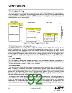
The memory organization of the CIP-51 System Controller is similar to that of a standard 8051. There are
two separate memory spaces: program memory and data memory. Program and data memory share the
same address space but are accessed via different instruction types. The memory organization of the
C8051F39x/37x device family is shown in Figure 17.1. Not shown in Figure 17.1 is 512 bytes of byte-
2
addressable EEPROM available on C8051F37x, accessible by SMBUS/I C (see Section 22).
PROGRAM/DATA MEMORY (FLASH)
DATA MEMORY (RAM)
C8051F390/1/2/3, C8051F370/1/4/5
0x4000
INTERNAL DATA ADDRESS SPACE
0xFF
Upper 128 RAM
(Indirect Addressing
Only)
Special Function
Register's
(Direct Addressing Only)
0x80
0x7F
0
F
16 kB FLASH
(Direct and Indirect
Addressing)
(In-System
Programmable in 512
Byte Sectors)
Lower 128 RAM
(Direct and Indirect
Addressing)
0x30
0x2F
Bit Addressable
0x20
0x1F
General Purpose
Registers
0x0000
0x00
EXTERNAL DATA ADDRESS SPACE
C8051F394/5/6/7
0x2000
0xFFFF
Same 1024 bytes as from
0x0000 to 0x03FF, wrapped
on 1024-byte boundaries
8 kB FLASH
0x0400
0x03FF
0x0300
0x02FF
(In-System
Programmable in 512
Byte Sectors)
Always Reads 0x00
XRAM - 768 Bytes
(accessable using MOVX
instruction)
0x0000
0x0000
C8051F398/9
0x1000
4 kB FLASH
(In-System
Programmable in 512
Byte Sectors)
0x0000
Figure 17.1. C8051F39x/37x Memory Map
Preliminary Rev. 0.71
91

 SILICON [ SILICON ]