C8051F39x/37x
11. 10-Bit Current Mode DACs (IDA0, IDA1, C8051F390/2/4/6/8 and
C8051F370/4 Only)
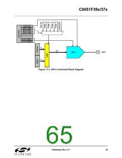
The C8051F390/2/4/6/8 and C8051F370/4 devices include two 10-bit current-mode Digital-to-Analog Con-
verters (IDACs). The maximum current output of the IDACs can be adjusted for three different current set-
tings; 0.5 mA, 1 mA, and 2 mA. The IDACs are enabled or disabled with the IDAnEN bit in the Control
Register for that IDAC (see SFR Definition 11.1 and SFR Definition 11.4). When IDAnEN is set to 0, the
IDAC output behaves as a normal GPIO pin. When IDAnEN is set to 1, the digital output drivers and weak
pullup for the IDAC pin are automatically disabled, and the pin is connected to the IDAC output. An internal
bandgap bias generator is used to generate a reference current for the IDAC whenever it is enabled. When
using an IDAC, the crossbar skip functionality should be enabled on the IDAC output pin, to force the
Crossbar to skip the output pin.
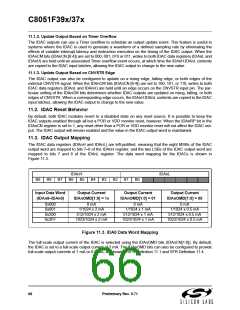
11.1. IDAC Output Scheduling
The IDACs feature a flexible output update mechanism which allows for seamless full-scale changes and
supports jitter-free updates for waveform generation. Three update modes are provided, allowing IDAC
output updates on a write to IDAnH, on a Timer overflow, or on an external pin edge.
11.1.1. Update Output On-Demand
In its default mode (IDAnCN.[6:4] = 111) the IDAC output is updated “on-demand” on a write to the high-
byte of the IDAC data register (IDAnH). It is important to note that writes to IDAnL are held in this mode,
and have no effect on the IDAC output until a write to IDAnH takes place. If writing a full 10-bit word to the
IDAC data registers, the 10-bit data word is written to the low byte (IDAnL) and high byte (IDAnH) data reg-
isters. Data is latched into the IDAC after a write to the IDAnH register, so the write sequence should be
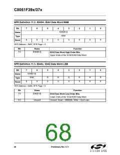
IDAnL followed by IDAnH if the full 10-bit resolution is required. The IDAC can be used in 8-bit mode by
initializing IDAnL to the desired value (typically 0x00), and writing data to only IDAnH (see Section 11.3 for
information on the format of the 10-bit IDAC data word within the 16-bit SFR space).
IDA0EN
IDA0CM2
IDA0CM1
IDA0CM0
IDA0OMD1
IDA0OMD0
8
10
IDA0
IDA0
2
Figure 11.1. IDA0 Functional Block Diagram
64
Preliminary Rev. 0.71

 SILICON [ SILICON ]