C8051F39x/37x
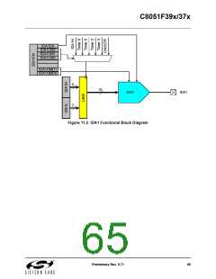
11.1.2. Update Output Based on Timer Overflow
The IDAC outputs can use a Timer overflow to schedule an output update event. This feature is useful in
systems where the IDAC is used to generate a waveform of a defined sampling rate by eliminating the
effects of variable interrupt latency and instruction execution on the timing of the IDAC output. When the
IDAnCM bits (IDAnCN.[6:4]) are set to 000, 001, 010 or 011, writes to both IDAC data registers (IDAnL and
IDAnH) are held until an associated Timer overflow event occurs, at which time the IDAnH:IDAnL contents
are copied to the IDAC input latches, allowing the IDAC output to change to the new value.
11.1.3. Update Output Based on CNVSTR Edge
The IDAC output can also be configured to update on a rising edge, falling edge, or both edges of the
external CNVSTR signal. When the IDAnCM bits (IDAnCN.[6:4]) are set to 100, 101, or 110, writes to both
IDAC data registers (IDAnL and IDAnH) are held until an edge occurs on the CNVSTR input pin. The par-
ticular setting of the IDAnCM bits determines whether IDAC outputs are updated on rising, falling, or both
edges of CNVSTR. When a corresponding edge occurs, the IDAnH:IDAnL contents are copied to the IDAC
input latches, allowing the IDAC output to change to the new value.
11.2. IDAC Reset Behavior
By default, both IDAC modules revert to a disabled state on any reset source. It is possible to keep the
IDAC outputs enabled through all but a POR or VDD monitor reset, however. When the IDAnRP bit in the
IDAnCN register is set to 1, any reset other than a POR or VDD monitor reset will not affect the IDAC out-
put. The IDAC output will remain enabled and the value in the IDAC output word is maintained.
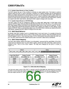
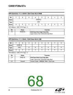
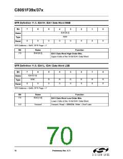
11.3. IDAC Output Mapping
The IDAC data registers (IDAnH and IDAnL) are left-justified, meaning that the eight MSBs of the IDAC
output word are mapped to bits 7–0 of the IDAnH register, and the two LSBs of the IDAC output word are
mapped to bits 7 and 6 of the IDAnL register. The data word mapping for the IDACs is shown in
Figure 11.3.
IDAnH
B6 B5
IDAnL
B9
B8
B7
B4
B3
B2
B1
B0
Input Data Word
(IDAn9–IDAn0)
Output Current
Output Current
Output Current
IDAnOMD[1:0] = 1x
IDAnOMD[1:0] = 01
IDAnOMD[1:0] = 00
0x000
0x001
0x200
0x3FF
0 mA
0 mA
0 mA
1/1024 x 2 mA
512/1024 x 2 mA
1023/1024 x 2 mA
1/1024 x 1 mA
512/1024 x 1 mA
1023/1024 x 1 mA
1/1024 x 0.5 mA
512/1024 x 0.5 mA
1023/1024 x 0.5 mA
Figure 11.3. IDA0 Data Word Mapping
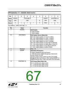
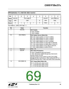
The full-scale output current of the IDAC is selected using the IDAnOMD bits (IDAnCN[1:0]). By default,
the IDAC is set to a full-scale output current of 2 mA. The IDAnOMD bits can also be configured to provide
full-scale output currents of 1 mA or 0.5 mA, as shown in SFR Definition 11.1 and SFR Definition 11.4.
66
Preliminary Rev. 0.71

 SILICON [ SILICON ]