C8051F39x/37x
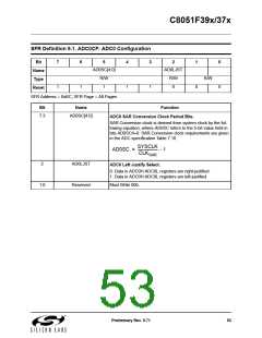
SFR Definition 9.4. ADC0CN: ADC0 Control
Bit
7
6
5
4
3
2
1
0
AD0EN
AD0TM
AD0INT AD0BUSY AD0WINT
AD0CM[2:0]
Name
Type
Reset
R/W
0
R/W
0
R/W
0
R/W
0
R/W
0
R/W
0
0
0
SFR Address = 0xE8; SFR Page = All Pages; Bit-Addressable
Bit
Name
Function
7
AD0EN
ADC0 Enable Bit.
0: ADC0 Disabled. ADC0 is in low-power shutdown.
1: ADC0 Enabled. ADC0 is active and ready for data conversions.
6
AD0TM
ADC0 Track Mode Bit.
0: Normal Track Mode: When ADC0 is enabled, tracking is continuous unless a con-
version is in progress. Conversion begins immediately on start-of-conversion event,
as defined by AD0CM[2:0].
1: Delayed Track Mode: When ADC0 is enabled, input is tracked when a conversion
is not in progress. A start-of-conversion signal initiates three SAR clocks of additional
tracking, and then begins the conversion. Note that there is not a tracking delay when
CNVSTR is used (AD0CM[2:0] = 100).
5
AD0INT
ADC0 Conversion Complete Interrupt Flag.
0: ADC0 has not completed a data conversion since AD0INT was last cleared.
1: ADC0 has completed a data conversion.
4
3
AD0BUSY
AD0WINT
ADC0 Busy Bit.
ADC0 Window Compare Interrupt Flag.
0: ADC0 Window Comparison Data match has not occurred since this flag was last
cleared.
1: ADC0 Window Comparison Data match has occurred.
2:0 AD0CM[2:
0]
ADC0 Start of Conversion Mode Select.
000: ADC0 start-of-conversion source is write of 1 to AD0BUSY.
001: ADC0 start-of-conversion source is overflow of Timer 0.
010: ADC0 start-of-conversion source is overflow of Timer 2.
011: ADC0 start-of-conversion source is overflow of Timer 1.
100: ADC0 start-of-conversion source is rising edge of external CNVSTR.
101: ADC0 start-of-conversion source is overflow of Timer 3.
110: ADC0 start-of-conversion source is overflow of Timer 4.
111: ADC0 start-of-conversion source is overflow of Timer 5.
Preliminary Rev. 0.71
55

 SILICON [ SILICON ]