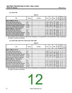
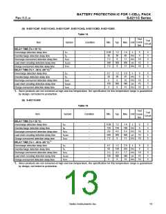
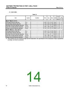
BATTERY PROTECTION IC FOR 1-CELL PACK
S-8211C Series
Rev.5.0_00
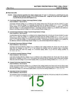
(7) Power-down Current Consumption
(Test Condition 5, Test Circuit 2)
The power-down current consumption (IPDN) is the current that flows through the VDD pin (IDD) under the set condition
of V1 = V2 = 1.5 V (overdischarge status).
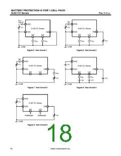
(8) Resistance between VM Pin and VDD Pin
(Test Condition 6, Test Circuit 3)
The resistance between VM pin and VDD pin (RVMD) is the resistance between VM pin and VDD pin under the set
conditions of V1 = 1.8 V, V2 = 0 V.
(9) Resistance between VM Pin and VSS Pin
(Test Condition 6, Test Circuit 3)
The resistance between VM pin and VSS pin (RVMS) is the resistance between VM pin and VSS pin under the set
conditions of V1 = 3.5 V, V2 = 1.0 V.
(10) CO Pin Resistance “H”
(Test Condition 7, Test Circuit 4)
The CO pin resistance “H” (RCOH) is the resistance at the CO pin under the set conditions of V1 = 3.5 V, V2 = 0 V,
V3 = 3.0 V.
(11) CO Pin Resistance “L”
(Test Condition 7, Test Circuit 4)
The CO pin resistance “L” (RCOL) is the resistance at the CO pin under the set conditions of V1 = 4.5 V, V2 = 0 V,
V3 = 0.5 V.
(12) DO Pin Resistance “H”
(Test Condition 8, Test Circuit 4)
The DO pin H resistance (RDOH) is the resistance at the DO pin under the set conditions of V1 = 3.5 V, V2 = 0 V,
V4 = 3.0 V.
(13) DO Pin Resistance “L”
(Test Condition 8, Test Circuit 4)
The DO pin L resistance (RDOL) is the resistance at the DO pin under the set conditions of V1 = 1.8 V, V2 = 0 V, V4 = 0.5 V.
(14) Overcharge Detection Delay Time
(Test Condition 9, Test Circuit 5)
The overcharge detection delay time (tCU) is the time needed for VCO to change from “H” to “L” just after the voltage
V1 momentarily increases (within 10 µs) from overcharge detection voltage (VCU) −0.2 V to overcharge detection
voltage (VCU) +0.2 V under the set condition of V2 = 0 V.
(15) Overdischarge Detection Delay Time
(Test Condition 9, Test Circuit 5)
The overdischarge detection delay time (tDL) is the time needed for VDO to change from “H” to “L” just after the voltage
V1 momentarily decreases (within 10 µs) from overcharge detection voltage (VDL) +0.2 V to overcharge detection
voltage (VDL) −0.2 V under the set condition of V2 = 0 V.
16
Seiko Instruments Inc.

 SII [ SEIKO INSTRUMENTS INC ]