BATTERY PROTECTION IC FOR 1-CELL PACK
S-8211C Series
Rev.5.0_00
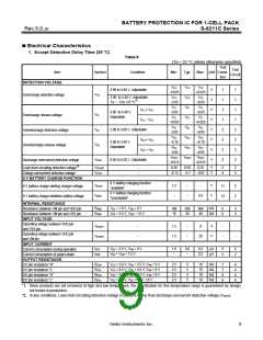
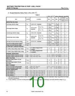
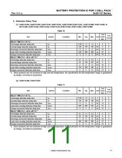
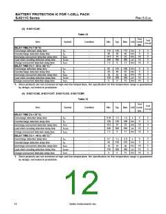
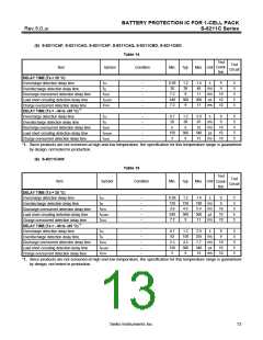
Electrical Characteristics
1. Except Detection Delay Time (25 °C)
Table 8
(Ta = 25 °C unless otherwise specified)
Test
Test
Item
Symbol
VCU
Condition
Min.
Typ.
Max. Unit Condi-
tion
Circuit
DETECTION VOLTAGE
VCU
VCU
VCU
VCL
VCU
3.90 to 4.40 V, Adjustable
V
V
V
V
V
V
V
V
1
1
1
1
2
2
2
3
1
1
1
1
2
2
2
2
−
0.025
VCU
+
0.025
VCU
Overcharge detection voltage
3.90 to 4.40 V, Adjustable,
*1
Ta =
−
5 to
+
55 °C
−
0.03
+
0.03
VCL
VCL
VCL
≠
VCU
3.80 to 4.40 V,
Adjustable
−
0.05
+
0.05
VCL
Overcharge release voltage
VCL
VCL
VCL
V
CL = VCU
−
0.025
VDL
+
0.025
VDL
VDL
VDL
2.00 to 3.00 V, Adjustable
Overdischarge detection voltage
Overdischarge release voltage
Discharge overcurrent detection voltage
−
0.05
+
0.05
VDU
VDU
VDU
VDIOV
0.50
VDU
VDU
≠
VDL
2.00 to 3.40 V,
Adjustable
−
0.10
+
0.10
VDU
VDU
VDU
V
DU = VDL
−
0.05
+
0.05
VDIOV
VDIOV
0.015
0.70
VDIOV
0.05 to 0.30 V, Adjustable
−
0.015
0.30
+
*2
VSHORT
VCIOV
−
−
V
V
3
4
2
2
Load short-circuiting detection voltage
Charge overcurrent detection voltage
−
0.13
−
0.1
−
0.07
0 V BATTERY CHARGE FUNCTION
0 V battery charging function
“available”
0 V battery charging function
“unavailable”
V0CHA
V0INH
1.2
−
−
−
V
V
0 V battery charge starting charger voltage
11
12
2
2
−
0.5
0 V battery charge inhibition battery voltage
INTERNAL RESISTANCE
Resistance between VM pin and VDD pin
Resistance between VM pin and VSS pin
INPUT VOLTAGE
RVMD
RVMS
VDD = 1.8 V, VVM = 0 V
VDD = 3.5 V, VVM = 1.0 V
k
k
Ω
Ω
100
10
300
20
900
40
6
6
3
3
Operating voltage between VDD pin
VDSOP1
VDSOP2
1.5
1.5
−
−
8
V
−
−
−
−
−
−
and VSS pin
Operating voltage between VDD pin
and VM pin
28
V
INPUT CURRENT
IOPE
IPDN
VDD = 3.5 V, VVM = 0 V
VDD = VVM = 1.5 V
1.0
−
3.0
−
5.5
0.2
µ
A
5
5
2
2
Current consumption during operation
Current consumption at power-down
OUTPUT RESISTANCE
CO pin resistance “H”
µA
RCOH
RCOL
RDOH
RDOL
VCO = 3.0 V, VDD = 3.5 V, VVM = 0 V
VCO = 0.5 V, VDD = 4.5 V, VVM = 0 V
VDO = 3.0 V, VDD = 3.5 V, VVM = 0 V
VDO = 0.5 V, VDD =VVM = 1.8 V
2.5
2.5
2.5
2.5
5
5
5
5
10
10
10
10
k
k
k
k
Ω
Ω
Ω
Ω
7
7
8
8
4
4
4
4
CO pin resistance “L”
DO pin resistance “H”
DO pin resistance “L”
*1. Since products are not screened at high and low temperature, the specification for this temperature range is guaranteed by design,
not tested in production.
*2. In any conditions, Load short-circuiting detection voltage (VSHORT) is higher than discharge overcurrent detection voltage (VDIOV).
Seiko Instruments Inc.
9

 SII [ SEIKO INSTRUMENTS INC ]