BATTERY PROTECTION IC FOR 1-CELL PACK
S-8211C Series
Rev.5.0_00
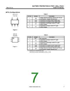
Pin Configurations
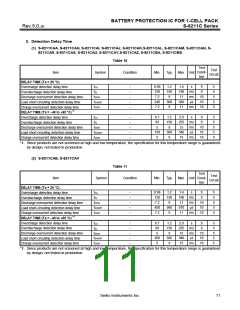
Table 5
SOT-23-5
Top view
Pin No.
1
Symbol
VM
Description
5
1
4
Voltage detection between VM pin and VSS pin
(Overcurrent / charger detection pin)
Connection for positive power supply input
Connection for negative power supply input
Connection of discharge control FET gate
(CMOS output)
2
3
VDD
VSS
4
DO
Connection of charge control FET gate
(CMOS output)
5
CO
2
3
Figure 2
SNT-6A
Top view
Table 6
Pin No.
1
Symbol
NC*1
Description
1
2
3
6
5
4
No connection
Connection of charge control FET gate
2
CO
(CMOS output)
Connection of discharge control FET gate
(CMOS output)
3
DO
4
5
VSS
VDD
Connection for negative power supply input
Connection for positive power supply input
Voltage detection between VM pin and VSS pin
(Overcurrent / charger detection pin)
Figure 3
6
VM
*1. The NC pin is electrically open.
The NC pin can be connected to VDD or VSS.
Seiko Instruments Inc.
7

 SII [ SEIKO INSTRUMENTS INC ]