BATTERY PROTECTION IC FOR 1-CELL PACK
S-8211C Series
Rev.5.0_00
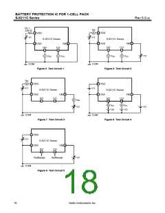
Test Circuits
Caution Unless otherwise specified, the output voltage levels “H” and “L” at CO pin (VCO) and DO pin (VDO) are
judged by the threshold voltage (1.0 V) of the N-channel FET. Judge the CO pin level with respect to
VVM and the DO pin level with respect to VSS.
(1) Overcharge Detection Voltage, Overcharge Release Voltage
(Test Condition 1, Test Circuit 1)
Overcharge detection voltage (VCU) is defined as the voltage between the VDD pin and VSS pin at which VCO goes
from “H” to “L” when the voltage V1 is gradually increased from the starting condition of V1 = 3.5 V. Overcharge
release voltage (VCL) is defined as the voltage between the VDD pin and VSS pin at which VCO goes from “L” to “H”
when the voltage V1 is then gradually decreased. Overcharge hysteresis voltage (VHC) is defined as the difference
between overcharge detection voltage (VCU) and overcharge release voltage (VCL).
(2) Overdischarge Detection Voltage, Overdischarge Release Voltage
(Test Condition 2, Test Circuit 2)
Overdischarge detection voltage (VDL) is defined as the voltage between the VDD pin and VSS pin at which VDO goes
from “H” to “L” when the voltage V1 is gradually decreased from the starting condition of V1 = 3.5 V, V2 = 0 V.
Overdischarge release voltage (VDU) is defined as the voltage between the VDD pin and VSS pin at which VDO goes
from “L” to “H” when the voltage V1 is then gradually increased. Overdischarge hysteresis voltage (VHD) is defined as
the difference between overdischarge release voltage (VDU) and overdischarge detection voltage (VDL).
(3) Discharge Overcurrent Detection Voltage
(Test Condition 3, Test Circuit 2)
Discharge overcurrent detection voltage (VDIOV) is defined as the voltage between the VM pin and VSS pin whose
delay time for changing VDO from “H” to “L” lies between the minimum and the maximum value of discharge
overcurrent delay time when the voltage V2 is increased rapidly (within 10 µs) from the starting condition of
V1 = 3.5 V, V2 = 0 V.
(4) Load Short-circuiting Detection Voltage
(Test Condition 3, Test Circuit 2)
Load short-circuiting detection voltage (VSHORT) is defined as the voltage between the VM pin and VSS pin whose
delay time for changing VDO from “H” to “L” lies between the minimum and the maximum value of load short-circuiting
delay time when the voltage V2 is increased rapidly (within 10 µs) from the starting condition of V1 = 3.5 V, V2 = 0 V.
(5) Charge Overcurrent Detection Voltage
(Test Condition 4, Test Circuit 2)
Charge overcurrent detection voltage (VCIOV) is defined as the voltage between the VM pin and VSS pin whose delay
time for changing VCO from “H” to “L” lies between the minimum and the maximum value of charge overcurrent delay
time when the voltage V2 is decreased rapidly (within 10 µs) from the starting condition of V1 = 3.5 V, V2 = 0 V.
(6) Operating Current Consumption
(Test Condition 5, Test Circuit 2)
The operating current consumption (IOPE) is the current that flows through the VDD pin (IDD) under the set conditions
of V1 = 3.5 V and V2 = 0 V (normal status).
Seiko Instruments Inc.
15

 SII [ SEIKO INSTRUMENTS INC ]