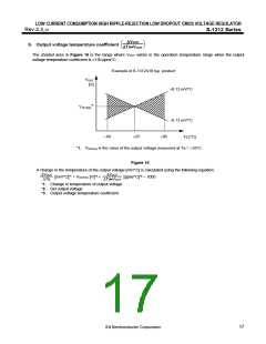
LOW CURRENT CONSUMPTION HIGH RIPPLE-REJECTION LOW DROPOUT CMOS VOLTAGE REGULATOR
Rev.2.3_01
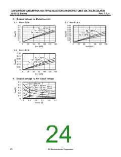
S-1312 Series
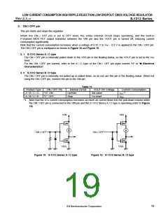
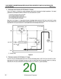
4. Discharge shunt function (S-1312 Series A / B type)
The S-1312 Series A / B type has a built-in discharge shunt circuit to discharge the output capacitance. The output
capacitance is discharged as follows so that the VOUT pin reaches the VSS level.
(1) The ON / OFF pin is set to OFF level.
(2) The output transistor is turned off.
(3) The discharge shunt circuit is turned on.
(4) The output capacitor discharges.
Since the S-1312 Series C / D type does not have a discharge shunt circuit, the VOUT pin is set to the VSS level
through several hundred kΩ internal divided resistors between the VOUT pin and the VSS pin. The S-1312 Series A / B
type allows the VOUT pin to reach the VSS level rapidly due to the discharge shunt circuit.
S-1312 Series
Output transistor : OFF
*1
VOUT
VIN
Discharge shunt circuit
: ON
Output
capacitor
*1
(CL)
ON / OFF
ON / OFF circuit
ON / OFF pin
: OFF
Current flow
GND
VSS
*1. Parasitic diode
Figure 20
5. Pull-down resistor (S-1312 Series A / C type)
The ON / OFF pin is internally pulled down to the VSS pin in the floating status, so the VOUT pin is set to the VSS level.
Note that the IC's current consumption increases as much as current flows into the pull-down resistor of 2.2 MΩ typ.
when the ON / OFF pin is connected to the VIN pin and the S-1312 Series A / C type is operating.
20

 SII [ SEIKO INSTRUMENTS INC ]