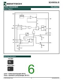
SC4905A/B
POWER MANAGEMENT
PRELIMINARY
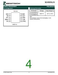
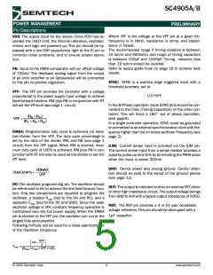
Pin Descriptions
Where VFF is the voltage at the VFF pin at a given Vin,
frequency is in Hertz, resistance in ohms, and capaci-
tance in farads.
VDD: The supply input for the device. Once VDD has ex-
ceeded the UVLO limit, the internal reference, oscillator,
drivers and logic are powered up. This pin should be by-
passed with a low ESR capacitance right at the IC pin to
minimize noise problems, and to ensure proper opera-
tion.
The recommended range if timing resistors is between
10 kohm and 500kohm and range of timing capacitors
is between 100pF and 1000pF. Timing resistors less
than 10 kohm should be avoided.
Refer to layout guide lines on page 16 to achieve best
results.
FB: Input to the PWM comparator with an offset voltage
of 700mV. The feedback analog signal from the output
of an error amplifier or an Optoisolator will be connected
to this pin to provide regulation.
SYNC: SYNC is a positive edge triggered input with a
threshold precisely set to
VFF: The VFF pin provides the controller with a voltage
proportional to the power supply input voltage to achieve
feed-forward function. RM plus RB in conjunction with RT
will set the Vff level (see page 1 circuit).
0.5*VFF
In the Bi-Phase operation mode SYNC pins should be con-
nected to the Cosc (Timing Capacitors) of the other con-
troller. This will force a 180° out of phase operation.
(see page9).
(
+
)
RT RB RM
R
R
M
B
=
VFF
(
+
+
)
In a single controller operation, SYNC could be grounded
or connected to an external synchronization clock with Fre-
quency higher than the on board oscillator Frequency (see
page 2).
DMAX: Programmable duty cycle is achieved via resis-
tive divider from the VFF. The duty cycle percentage is
set by the ratio of the divider RM, and RB (see page 1
circuit) from the VFF signal. When RM is shorted, maxi-
mum duty cycle of 100% is achieved. RM plus RB in con-
junction with RT will also be used as the divider to set the
Vff level.
ILIM: Current sense input is provided via the ILIM pin.
The current sense input from a sense resistor provides a
pulse by pulse current limit by terminating the PWM pulse
when the input is above 200mV.
GND: Device power and analog ground. Careful atten-
tion should be paid to the layout of the ground planes
(see page 12).
VDMAX
DutyCycle%=
VFF
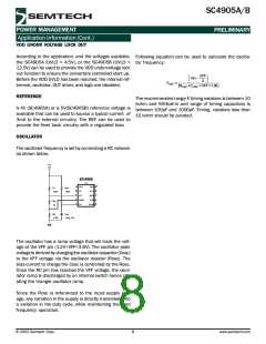
RC: The oscillator programming pin. The oscillator should
be referenced to Vin to achieve the line feed forward func-
tion. Only two components are required to program the
OUT: The output is intended to drive an external FET driver
or other high impedance circuit. The output voltage swings
from GND to Vref with a typical output impedance of 500Ω.
oscillator, a resistor R (tied to the Vin and RC), and a
OSC
capacitor C (tied to the RC and GND). Since the peak
OSC
REF: The REF pin provides a 4 or 5V user accessible
oscillator voltage is VFF, constant frequency operation is
maintained over the full power supply. When the DMAX
pin is shorted to the VFF pin, the oscillator can run at the
largest duty cycle possible.
voltage reference. This pin should be decoupled with a
1µF capacitor.
Following formula can be used for a close approximation
of the Oscillator Frequency.
VFF
Vin−
2
F
≅
R
OSC
(
• C
• VFF•1.05
)
OSC
OSC
2002 Semtech Corp.
5
www.semtech.com

 SEMTECH [ SEMTECH CORPORATION ]