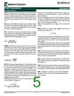
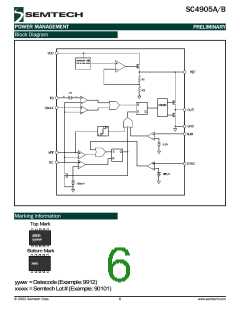
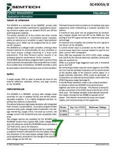
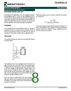
SC4905A/B
POWER MANAGEMENT
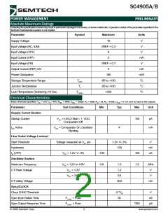
Absolute Maximum Ratings
PRELIMINARY
Exceeding the specifications belowmay result in permanent damage to the device, or device malfunction. Operation outside of the parameters specified in the
Electrical Characteristics section is not implied.
Parameter
Symbol
Maximum
Units
SupplyVoltage
18
V
V
Input Voltage (RC, ILIM)
Input Voltage (VFF)
VREF + 0.3
6
2
V
Input Current (VFF)
mA
V
Input Voltage (FB)
VREF + 0.7
5
Output Current (REF) DC
Power Dissipation
mA
mW
°C
°C
°C
180
Storage Temperature Range
JunctionTemperature
Lead Temperature (Soldering) 10 Sec.
T
-65 to +150
-55 to +150
+300
STG
T
J
T
LEAD
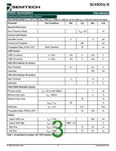
Electrical Characteristics
Unless otherwise specified, V = 12V, V = 48V, R = 499k, C = 220pF, R = 280k, R = 2k, R = 8.25k, C = 0.1uF, and no load on the outputs.
M
DD
IN
OSC
OSC
T
B
VDD
Parameter
Test Conditions
Min
Typ
Max
Unit
Supply Curent Section
Startup Current
V
DD
= UVLOStart - 1, VDD
100
µA
Comparator Off
= Comparator On, Oscillator
DD
I Active
DD
V
4
mA
Running
Line Under Voltage Lockout
Start Threshold
Voltage measured at V pin
FF
1.2V +/- 3%
100
V
Hysteresis
mV
nA
I (VFF)
IB
V = 1.2V +/- 3%
FF
-100
100
Oscillator Section
MaximumFrequency
CTPeak Voltage
V = 1.2V to 4.8V
FF
0.8
1.0
1.2
3.6
200
1.2
MHz
V
V = 1.2V
FF
V = 3.6V
FF
V
CTValleyVoltage
mV
Sync/CLOCK
Clock SYNC Threshold
Sync Input Detect Time
Sync Output Response Time
2002 Semtech Corp.
.5 *V
V
FF
F
> Fosc
< Fosc
50
nS
µS
SYNC
F
SYNC
TBD
2
www.semtech.com

 SEMTECH [ SEMTECH CORPORATION ]