SC4905A/B
POWER MANAGEMENT
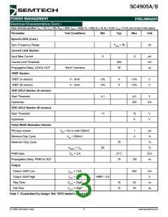
Electrical Characteristics (Cont.)
PRELIMINARY
Unless otherwise specified, V = 12V, V = 48V, R = 499k, C = 220pF, R = 280k, R = 2k, R = 8.25k, C = 0.1uF, and no load on the outputs.
M
DD
IN
OSC
OSC
T
B
VDD
Parameter
Test Conditions
Min
Typ
Max
Unit
Sync/CLOCK (Cont.)
Sync Frequency Range
Current Limit Section
Input Bias Current
F
OSC
+ 50
Hz
0
-2
µA
mV
ns
Current Limit Threshold
200
35
PropagationDelay, ILIM to OUT
VREF Section
50mV Overdrive
VREF (A version)
0 - 5mA
0 - 5mA
-3%
-3%
4
5
+3%
+3%
V
V
VREF (B version)
VDD UVLO Section (A version)
Start Threshold
4.1
4.5
V
Hysteresis
300
mV
VDD UVLO Section (B version)
Start Threshold
11
12
4
V
V
Hysteresis
Pulse Width Modulator Section
FB Input current
V = 0V to Vref+300mV
FB
1
0
uA
%
MinimumDuty Cycle
MaximumDuty Cycle
V < 500mV
FB
78
%
V
DMAX
= V
90
%
FF
PWM Gain
V = 3.6
FF
27.7
75
%/V
ns
PropagationDelay, PWM to OUT
120
500
Output
Output VSAT Low
Output VSAT High
Rise Time
I
I
= 1mA
mV
V
OUT
= 1mA
VREF - 0.5
OUT
C
= 20pF
= 20pF
10
10
25
25
ns
ns
OUT
Fall Time
C
OUT
Note 1: Guaranteed by design. Not 100%tested in production.
2002 Semtech Corp.
3
www.semtech.com

 SEMTECH [ SEMTECH CORPORATION ]