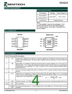
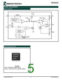
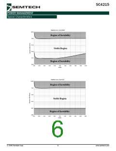
SC4215
POWER MANAGEMENT
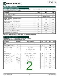
Absolute Maximum Ratings
Exceeding the specifications below may result in permanent damage to the device, or device malfunction. Operation outside of the parameters specified in
the Electrical Characteristics section is not implied.
Parameter
Symbol
Max
Units
V
Vin, EN, Vo, ADJ to GND
Power Dissipation
7
PD
Internally Limited
W
Thermal Resistance Junction to Ambient
SOIC-8EDP(1)
36
°C/W
θJA
Thermal Resistance Junction to Case
SOIC-8EDP(1)
θJC
TA
5.5
-40 to +85
-40 to +125
-65 to +150
300
°C/W
°C
Operating Ambient Temperature Range
Operating Junction Temperature Range
Storage Temperature Range
TJ
°C
TSTG
TLEAD
VESD
°C
Lead Temperature (Soldering) 10 Sec.
°C
ESD Rating (Human Body Model)
2
kV
Note: (1) 2 square inch of FR-4, double sided, 1 oz. minimum copper weight.
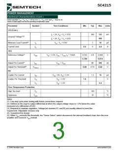
Electrical Characteristics
Unless specified: V = VIN. V = 1.6V to 5.5V, VO = VIN -0.5V, and IO = 10µA to 2A.
Values in bold applEyNover theINfull operating temperature range.
Parameter
Symbol
Test Conditions
Min
Typ
Max
Units
VIN
Supply Voltage Range
Quiescent Current
VIN
IQ
1.6
5.5
1.75
50
V
VIN = 3.3V
0.75
10
mA
µA
VIN = 5.5V, VEN = 0V
VO
Output Voltage(1)
(Fixed Voltage, VADJ = 0)
Line Regulation(1)
Load Regulation(1)
Dropout Voltage(1)(2)
VO
VIN = VO + 0.5V, IO = 10mA
Full IOUT and VIN range
IO = 10mA
-2%
VO
+2%
+3%
0.4
V
-3%
REG(LINE)
REG(LOAD)
VD
0.2
0.5
90
%/V
%
IO = 10mA to 2A
IO = 1A
1.0
300
400
400
500
mV
IO = 1.5A
200
mV
2006 Semtech Corp.
2
www.semtech.com

 SEMTECH [ SEMTECH CORPORATION ]