STK672-120-SL-E
Precautions
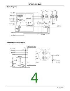
• To minimize noise in the 5V system, locate the ground side of capacitor CO2 in the above circuit as close as
possibleto pin 1 of the IC.
• Insert resistor RO3 (47 to 100Ω) so that the discharge energy from capacitor CO4 is not directly applied to the
CMOS-IC in this hybrid device. If the diode D1 has Vf characteristics with Vf less than or equal to 0.6V (when If =
0.1A), this will be smaller than the CMOS IC input pin diode Vf. If this is the case RO3 may be replaced with a short
without problem.
• Standard or HC type input levels are used for the pin 7, 8, and 9 inputs.
• If open-collector type circuits are used for the pin 7, 8, and 9 inputs, these circuit will be in the high-impedance state
for high level inputs. As a result, chopping circuit noise may cause the input circuits to operate incorrectly. To prevent
incorrect operation due to such noise, capacitors with values between 470 and 1000pF must be connected between
pins 7 and 11, 8 and 11, and 9 and 11. (A capacitor with a value between 470 and 1000pF must be connected between
pins 6 and 11 as well if an open-collector output IC is used for the RESETB pin (pin 6) input.)
• Taking the input bias current (I ) characteristics into account, the resistor RO1 must not exceed 100kΩ.
IB
• The following circuit (for a lowered current of over 0.2A) is recommended if the application needs to temporarily
lower the motor current. Here, a value of close to 100kΩ must be used for resistor RO1 to make the transistor output
saturation voltage as low as possible.
5V
5V
RO1
RO1
Vref
Vref
RO2
R3
R3
RO2
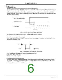
Input Pin Functions (CMOS input levels)
Pin
Pin No.
Function
Reference clock for motor phase current switching
Excitation mode selection
Input conditions when operating
CLOCK
9
8
Operates on the rising edge of the signal
MODE
CWB
Low: 2-phase excitation
High: 1-2 phase excitation
Low: CW (forward)
7
6
Motor direction switching
High: CCW (reverse)
RESETB
System reset and A, AB, B, and BB outputs cutoff.
Applications must apply a reset signal for at least 20μs
when power is first applied.
A reset is applied by a low level
(1) A simple reset function is formed from D1, CO4, and RO3 in this application circuit. With the CLOCK input
held low, when the 5V supply voltage is brought up a reset is applied if the motor output phases A and BB are
driven. If the 5V supply voltage rise time is slow (over 50ms), the motor output phases A and BB may not be driven.
Increase the value of the capacitor CO4 and check circuit operation again.
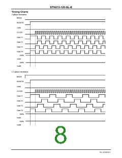
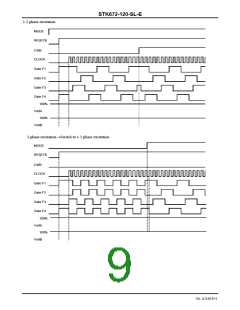
(2) See the timing chart for the concrete details on circuit operation.
No. A2140-5/11

 SANYO [ SANYO SEMICON DEVICE ]