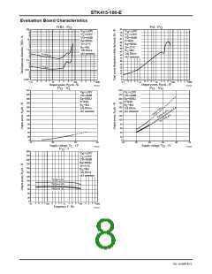
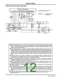
STK415-100-E
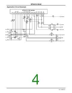
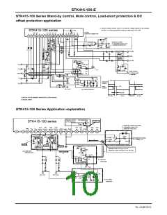
The protection circuit application for the STK415-100sr consists of the following blocks (blocks (1) to (4)).
(1) Standby control circuit block
(2) Load short-circuit detection block
(3) Latch-up circuit block
(4) DC voltage protection block
1) Standby control circuit block
Concerning pin 17 reference voltage VST
<1> Operation mode
The switching transistor of the predriver IC turns on when the pin 17 reference voltage, VST, becomes greater
than or equal to 2.5V, placing the amplifier into the operation mode.
Example: When VST (min.) = 2.5V
I1 is approximately equal to 0.40mA since VST = (*2) × IST + 0.6V → 2.5V = 4.7kΩ × IST + 0.6V.
<2> Standby mode
The switching transistor of the predriver IC turns off when the pin 17 reference voltage, VST, becomes lower
than or equal to 0.6V (typ. 0V), placing the amplifier into the standby mode.
Example: When VST = 0.6V
I1 is approximately equal to 0mA since VST = (*2) × IST + 0.6V → 0.6V = 4.7kΩ × IST + 0.6V.
(*1) Limiting resistor
Determine the value of R1 so that the voltage VST applied to the standby pin (pin 17) falls within the rating
(+2.5V to 5.5V (typ. 3.0V)).
(*2) The standby control voltage must be supplied from the host including microcontrollers.
(*3) A 4.7kΩ limiting resistor is also incorporated inside the hybrid IC (at pin 17).
2) Load short-circuit detection block
Since the voltage between point B and point C is less than 0.6V in normal operation mode (V
TR2) is not activated, the load short-circuit detection block does not operate.
< 0.6V) and TR1 (or
BE
When a load short-circuit occurs, however, the voltage between point B and point C becomes larger than 0.6V,
causing TR1 (or TR2) to turn on (V
> 0.6V), and current I2 to flows.
BE
3) Latch-up circuit block
TR3 is activated when I2 is supplied to the latch-up circuit.
When TR3 turns on and current I3 starts flowing, VST goes down to 0V (standby mode), protecting the power
amplifier.
Since TR3 and TR4 configure a thyristor, once TR3 is activated, the IC is held in the standby mode.
To release the standby mode and reactivate the power amplifier, it is necessary to set the standby control voltage (*2)
temporarily low (0V). Subsequently, when the standby control is returned to high, the power amplifier will become
active again.
(*4) The I3 value varies depending on the supply voltage. Determine the value of R2 using the formula below, so that
I1 is equal to or less than I3.
I1 ≤ I3 = V /R2
CC
4) DC offset protection block
The DC offset protection circuit is activated when 0.5V (typ) voltage is applied to either "OUT CH1" or "OUT
CH2," and the hybrid IC is shut down (standby mode).
To release the IC from the standby mode and reactivate the power amplifier, it is necessary to set the standby control
voltage temporarily low (0V).
Subsequently, when the standby control is returned to high (+5V, for example), the power amplifier will become
active again.
The protection level must be set using the 82kΩ resistor. Furthermore, the time constant must be determined using
22μ//22μ capacitors to prevent the amplifier from malfunctioning due to the audio signal.
No. A1469-11/12

 SANYO [ SANYO SEMICON DEVICE ]