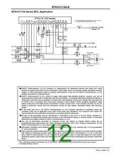
STK415-100-E
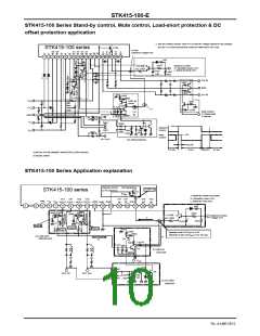
STK415-100 Series Stand-by control, Mute control, Load-short protection & DC
offset protection application
*1 Set the limiting resistor value R1 so that the voltage applied to the standby
pin (pin 17) never exceeds the maximum rated value VST max.
4.7kΩ
STK415-100 series
#17pin
reference voltage VST
+OFF -OFF
OUT OUT OUT OUT
Ch1+ Ch1- Ch2+ Ch2-
NF
Ch2
IN
NF
Ch1 Ch1
IN
Ch2
ST-
BY
-V
+V
-Pre -V
+V
SUB
+Pre GND
SET
SET
L
L
H
H
1
2
3
4
6
7
8
9 10 11 12 13 14 15 16 17 18 19
5
1kΩ
6.8kΩ
33kΩ
Stand-by Control
H: Operation Mode (+5V)
L: Stand-by Mode (0V)
(*1) R30
ex) 3.3kΩ
47μF
/10V
2kΩ
GND
*3 *3
6.8kΩ
Ch2 IN
*2
10kΩ
GND
10kΩ
10kΩ
2.2kΩ
Ch1 IN
22kΩ
1kΩ
*2
56kΩ
Latch up
circuit
+V
H
Load
Short
Protection
circuit
0.1μF
10kΩ
+V
L
V1
Mute Control
H: Single Mute
L: Normal
(*4)
R2
Ch2 OUT
GND
100kΩ
-V
L
GND
GND
82kΩ
+5V
Stand-by
Control
-V
H
100
kΩ
22μF
22μF
82kΩ
+5V
Mute
Control
Ch1 OUT
DC offset protection
MUTE
PLAY
ST-BY
MUTE
ST-BY
*2 METAL PLATE CEMENT RESISTOR 0.22Ω 10%(5W)
*3 DIODE 3A/60V
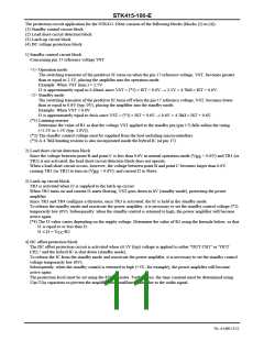
STK415-100 Series Application explanation
Stand-by Circuit
in Pre Driver IC
SW transistor
4.7kΩ (*3)
STK415-100 series
ΔV
BE
1) Stand-by control circuit part
H: Operation mode (+5V)
L: Stand-by mode (0V)
Ch1
Ch1
Ch1
Ch2
Ch2
Ch1
Ch2
Ch2
IN
-PRE -V
+V
+PRE
12
GND
NF STBY
OUT(+) OUT(-) OUT(+) OUT(-)
SUB
13
IN
NF
H
H
1
4
5
6
7
8
10
11
14
15
16
17
18
19
9
1kΩ
6.8kΩ
6.8kΩ
56kΩ
33kΩ
56kΩ
(*1) R30
ex) 3.3kΩ
Tr5
Stand-By Control
Voltage VST
I1
2kΩ
47μF
Tr1
Tr2
Point.B
Point.B
Point.C
I2
Point.C
22kΩ
56kΩ
Operate mode (VST
)≥ 2.5V
)< 0.6V (0V typ)
OFF
Stand-By mode (VST
ON
(2) Load short
detection part
I3
Tr4
(*4) R2
1kΩ
0.1μF
10kΩ
Tr3
(3) Latch-up
circuit part
100kΩ
-V
CC
Tr5
82kΩ
Tr6
OUT Ch1
OUT Ch2
22μF
82kΩ 22μF
100
kΩ
(4) DC offset
protection
No. A1469-10/12

 SANYO [ SANYO SEMICON DEVICE ]