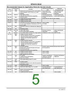
STK415-100-E
Recommended Values for Application Parts (for the test circuit)
Recommended
Larger than Recommended
Smaller than
Recommended Value
Power switching circuit
activates at higher
Symbol
Description
Value
Value
R01, R02
1.5kΩ
Determine the current flowing into the power switching
Power holding circuit
remains active at lower
frequencies.
circuit (comparator), (3mA to 10mA at V power
H
switching)
frequencies.
R03, R04
R05, R06
100Ω/1W
56kΩ
Ripple filtering resistors
Decreased pass-through
current at high frequencies.
VN offset
Increased pass-through
current at high frequencies.
(Used with C05 and C06 to form a ripple filter.)
Input bias resistors
(Virtually determine the input impedance.)
Oscillation prevention resistor
(Ensure R05=R18, R06=R19 when changing.)
R08, R09
R11, R12
R14,R15
4.7Ω/1W
4.7Ω
-
-
-
-
Oscillation prevention resistor
560Ω
Used with R18 and R19 to determine the voltage gain
VG. (VG should desirably be determined by the R14
and R15 value.)
Likely to oscillate
(VG<40dB)
None
R18, R19
56kΩ
1kΩ
Used with R14 and R15 to determine the voltage gain
VG.
-
-
-
R21, R22
R24, R26
Input filtering resistor
-
0.22Ω 10%,
5W
Output emitter resistors
Decrease in maximum
output power
Likely to cause thermal-
runaway.
(Use of cement resistor is desirable)
R30
Remarks *7
Use a limiting resistor according to the voltage applied to the standby pin so that it remains within the rating.
C01, C02
100μF/
Oscillation prevention capacitors.
100V
• Insert the capacitors as close to the IC as possible to
decrease the power impedance for reliable IC
operation (use of electrolytic capacitors are
desirable).
-
-
-
-
C03, C04
C05, C06
100μF/
Oscillation prevention capacitors.
• Insert the capacitors as close to the IC as possible to
decrease the power impedance for reliable IC
operation (use of electrolytic capacitors are
desirable).
50V
100μF/
Decoupling capacitors.
Increase in ripple components that pass into the input side
from the power line.
100V
Eliminate ripple components that pass into the input
side from the power line.
(Used with R03 and R04 to form a ripple filter.)
Oscillation prevention capacitor
C07, C08
C10, C11
3pF
Likely to oscillate
Likely to oscillate
0.1μF
Oscillation prevention capacitor
(Mylar capacitors are recommended.)
NF capacitor
C13, C14
22μF/
Increase in low-frequency
voltage gain, with higher
pop noise at power-on.
Decrease in low-frequency
voltage gain
10V
(Changes the low cutoff frequency;
ex/f =1/2π •C13•R14)
L
C16, C17
C19, C20
2.2μF/
50V
Input coupling capacitor (block DC current)
-
-
-
470pF
Input filter capacitor
(Used with R21 and R22 to form a filter that suppresses
high-frequency noises.)
-
C22, C23
D01, D02
100pF
15V
Oscillation prevention capacitor
Likely to oscillate.
Determine the offset voltage at V ↔V power.
Decreased distortion at
power switching time
Increased distortion at
power switching time.
L
H
D03, D04
L01, L02
3A/60V
Reverse current prevention diodes
(FRD is recommended.)
-
-
3μH
Oscillation prevention inductance
None
Likely to oscillate.
No. A1469-5/12

 SANYO [ SANYO SEMICON DEVICE ]