LC89057W-VF4A-E
8.4 AC Characteristics
Table 8.4: AC Characteristics at Ta=-30 to 70°C, AV =DV =3.0 to 3.6V, AGND=DGND=0V
DD
DD
Ratings
Parameter
Symbol
Conditions
Unit
min
typ
max
195
RX0 to RX6 sampling frequency
XIN clock frequency
XIN clock frequency
RMCK clock frequency
RMCK clock jitter
f
f
f
f
28
8
kHz
MHz
MHz
MHz
ps
RFS
1
2
8-4-1
8-4-2
12.288
24.576
19
30
XF
20
4
XF
100
RCK
tj
t
200
RMCK, RBCK delay
RBCK, RDATA delay
RMCK, SBCK delay
SBCK, RDATA delay
TMCK input pulse width
RX*, TMCK delay
10
10
10
10
ns
MBO
t
t
t
t
t
t
t
t
t
t
t
ns
BDO
MBO
BDO
WMI
RDI
8-4-3
8-4-4
ns
ns
10
ns
1/4TMCK
195
ns
TBCK input pulse width
TLRCK sampling frequency
TBCK, TDATA setup
TBCK, TDATA hold
40
28
ns
WBI
TFS
DSI
kHz
ns
20
20
ns
DHI
TMCK, TBCK delay
TBCK, TDATA delay
8-4-5
10
10
ns
MBI
BDI
ns
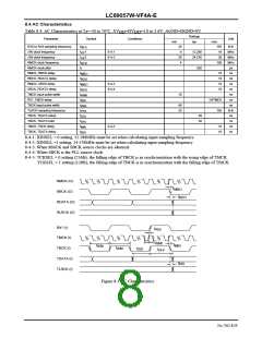
8-4-1: XINSEL = 0 setting, 12.288MHz must be set when calculating input sampling frequency
8-4-2: XINSEL =1 setting, 24.576MHz must be set when calculating input sampling frequency
8-4-3: When RMCK and SBCK source clocks are identical
8-4-4: When SBCK is the PLL source clock
8-4-5: TCKSEL = 0 setting (256fs), the falling edge of TBCK is in synchronization with the rising edge of TMCK.
TCKSEL = 1 setting (128fs), the falling edge of TBCK is in synchronization with the falling edge of TMCK.
RMCK (O)
t
MBO
RBCK (O)
RDATA (O)
RLRCK (O)
t
BDO
RX* (I)
t
t
RDI
TMCK (I)
TBCK (I)
TDATA (I)
TLRCK (I)
WMI
t
t
MBI
WBI
t
t
WBI
DSI
t
DHI
t
BDI
Figure 8.1 AC Characteristics
No.7202-8/59

 SANYO [ SANYO SEMICON DEVICE ]