LC89057W-VF4A-E
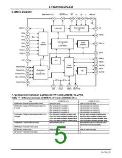
6. Block Diagram
EMPHA/UO/CO
AUDIO/VO
33
INT CL CE
35 48 39
CI
XMODE
41
32
38
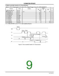
Microcontroller
I/F
RXOUT
1
DO
Cbit, Ubit
37
RX0
RX1
2
3
RERR
36
21
RX2
4
Demodulation
&
Lock detect
Input
Selector
Data
Selector
RX3
RDATA
SDIN
5
RX4
8
RX5/VI
RX6/UI
9
24
10
RMCK
RBCK
RLRCK
SBCK
16
17
20
22
23
LPF
13
PLL
Clock
Selector
TMCK/PIO0
TBCK/PIO1
TLRCK/PIO2
TDATA/PIO3
44
45
46
47
Modulation
1/N
or
SLRCK
Parallel Port
TXO/PIOEN
48
29
28
27
34
XIN
XOUT
XMCK CKST/PB
7. Comparison between LC89057W-VF4 and LC89057W-VF4A
Table 7.1 Difference between LC89057W-VF4 and LC89057W-VF4A
Item
LC89057W-VF4
256fs clock input
LC89057W-VF4A
256fs or 512fs clock input
DIR function: External synchronization mode
DIR function: Setting of RERR wait time after PLL
is locked
After preamble B is counted 6.
After preamble B is counted 3.
After preamble B is counted 12.
After preamble B is counted 6.
After preamble B is counted 24.
After preamble B is counted 12.
After preamble B is counted 48.
After preamble B is counted 24.
DIR function: Setting of clock wait time after PLL is
unlocked
50μs from when oscillation amplifier starts
100μs from when oscillation amplifier starts
200μs from when oscillation amplifier starts
400μs from when oscillation amplifier starts
Microcontroller read out
0μs from when oscillation amplifier starts
50μs from when oscillation amplifier starts
100μs from when oscillation amplifier starts
200μs from when oscillation amplifier starts
Microcontroller read out or terminal output
(full decode processing possible)
DIR function: Channel status bit output
DIR function: Preamble B info output
DIT function: System clock
×
{
256fs clock input
256fs or 128fs clock input
DIT function: Preamble B info output
×
{
No.7202-5/59

 SANYO [ SANYO SEMICON DEVICE ]