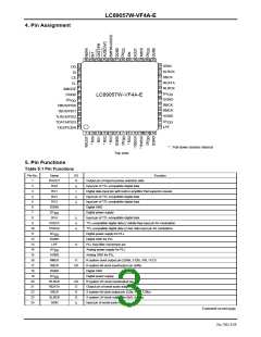
LC89057W-VF4A-E
Continued from preceding page.
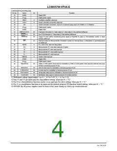
Pin No.
25
Name
I/O
Function
DGND
Digital GND
26
DV
DD
Digital power supply
27
XMCK
XOUT
XIN
O
O
I
Oscillation amplifier output pin
Quartz resonator connection output pin
28
29
Quartz resonator connection, input pin of external supply clock (24.576MHz or 12.288MHz)
Digital power supply
30
DV
DD
31
DGND
Digital GND
32
EMPHA/UO/CO
I/O
I/O
I/O
Emphasis information || U data output || C data output || Chip address setting pin
Non-PCM detection || V flag output || Chip address setting pin
AUDIO
33
/VO
/PB
CKST
34
Output of clock switch transitional period signal || Preamble B output || Demodulation master or slave
function switch pin
INT
35
I/O
Interrupt output for Microcontroller (Possible to select an interrupt factor.) || Modulation or general-purpose
I/O switch pin
36
37
38
39
40
41
42
43
44
RERR
DO
O
O
I5
I5
I5
I5
PLL clock error, data error flag output
Microcontroller I/F, read data output pin (3-state)
Microcontroller I/F, write data input pin
Microcontroller I/F, chip enable input pin
Microcontroller I/F, clock input pin
System reset input pin
DI
CE
CL
XMODE
DGND
Digital GND
DV
DD
Digital power supply
TMCK/PIO0
I/O
256fs or 128fs system clock input for modulation || 256fs or 512fs system clock input for external clock sync
function || General-purpose I/O pin
45
46
47
48
TBCK/PIO1
TLRCK/PIO2
TDATA/PIO3
TXO/PIOEN
I/O
I/O
I/O
O/I
64fs bit clock input for modulation || General-purpose I/O pin
fs clock input for modulation || General-purpose I/O pin
serial audio data input for modulation || General-purpose I/O pin
Modulation data output || General-purpose I/O enable input pin
1) Withstand voltage input/output: I or O = -0.3 to 3.6V, I5 = -0.3 to 5.5V
2) Pins 32 and 33 are input pins for chip address setting, when pin 41 = "L".
3) Pin 34 is a demodulation function master or an input pin for slave setting, when pin 41 = "L".
4) Pin 35 is a modulation function or an input pin for general-purpose I/O function switch setting, when pin 41 = "L".
5) ON/OFF for all power supplies must be done at the same timing as a latch-up countermeasure.
No.7202-4/59

 SANYO [ SANYO SEMICON DEVICE ]