LC89057W-VF4A-E
9. Initial System Settings
9.1 System Reset (XMODE)
•
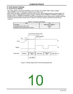
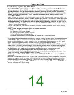
The system operates correctly when XMODE is set to "H" after 3.0V or higher supply voltage is applied.
When XMODE is set to "L" after power is turned on, the system is reset.
•
•
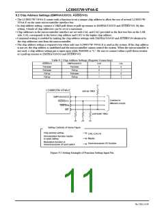
When setting chip address, demodulation function master or slave, and modulation function or general-purpose I/O
____________
__________
______
function, connect a 10kΩ pull-down or pull-up resistor to EMPHA/UO/CO, AUDIO/VO, CKST/PB, and INT pins.
____________
__________
______
If EMPHA/UO/CO, AUDIO/VO, CKST/PB, and INT are not pulled up or down, their pin state is unstable at the time
of input. Consequently proper setting cannot be realized. For these pins, pull-up or pull-down resistor must be
connected.
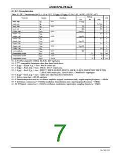
Table 9.1: Pin Names and Settings
Setting
Pins
________
Chip address
EMPHA/UO/CO, AUDIO/VO
_______
CKST/PB
____
Demodulation function master or slave
Modulation function or general-purpose I/O function
INT
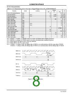
Normal system operation range
Setting completed
3.3V
3.0V
DV
DD
XMODE
Setting input
Setting input
state
Set pin state
Undefined
Output state
Output state
state
min. 200μs
Figure 9.1 Setting Timing Chart of Function Setting Input Pins
No.7202-10/59

 SANYO [ SANYO SEMICON DEVICE ]