LC89057W-VF4A-E
12.2.3 Channel status data write
•
For channel status data write with the modulation function, set the CCB address to 0xE9.
DI0 to DI7 are not channel status bits. Be sure to input a chip address to DI0 and DI1. Input "0" to DI2, DI3, and DI7
because they are reserved by the system. Write length of the channel status data is determined with DI4 to DI6. This
setting is possible up to 48 bits in units of 8 bits.
After CE rises, input a clock combined DI0 to DI7 and write data length to CL clock to make CE “L”. For example, if
you write data up to the bit 15 by DI4 to DI6, CL must be 24 clocks while CE is rising. If this setting goes wrong,
correct writing is not expected.
•
•
•
Input data is written from preamble B where CE has become "L".
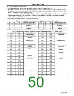
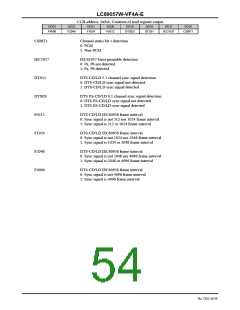
Table 12.3 Relation between Setting Register of Input Data Length and Data Length
DI6
0
DI5
0
DI4
Feasible Data Range for Input
DI6
DI5
DI4
Feasible Data Range for Input
0
Bit 0 to bit 7
1
0
0
Bit 0 to bit 39
0
0
1
Bit 0 to bit 15
1
0
1
Bit 0 to bit 47
0
1
0
Bit 0 to bit 23
1
1
0
Reserved
0
1
1
Bit 0 to bit 31
1
1
1
Reserved
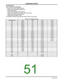
Table 12.4 Input Setting -Setting of Modulation Function Channel Status Data- (CCB address : 0xE9)
Register
Bit No.
CAL
CAU
0
Description
Lower chip address
Higher chip address
Reserved
Register
DI28
DI29
DI30
DI31
DI32
DI33
DI34
DI35
DI36
DI37
DI38
DI39
DI40
DI41
DI42
DI43
DI44
DI45
DI46
DI47
DI48
DI49
DI50
DI51
DI52
DI53
DI54
DI55
Bit No.
Bit 20
Bit 21
Bit 22
Bit 23
Bit 24
Bit 25
Bit 26
Bit 27
Bit 28
Bit 29
Bit 30
Bit 31
Bit 32
Bit 33
Bit 34
Bit 35
Bit 36
Bit 37
Bit 38
Bit 39
Bit 40
Bit 41
Bit 42
Bit 43
Bit 44
Bit 45
Bit 46
Bit 47
Description
DI0
DI1
Channel number
DI2
DI3
0
DI4
0
Data length setting
Sampling frequency
DI5
0
DI6
0
DI7
0
Reserved
Application
Control
DI8
Bit 0
Bit 1
Bit 2
Bit 3
Bit 4
Bit 5
Bit 6
Bit 7
Bit 8
Bit 9
Bit 10
Bit 11
Bit 12
Bit 13
Bit 14
Bit 15
Bit 16
Bit 17
Bit 18
Bit 19
Clock accuracy
Not defined
DI9
DI10
DI11
DI12
DI13
DI14
DI15
DI16
DI17
DI18
DI19
DI20
DI21
DI22
DI23
DI24
DI25
DI26
DI27
Word length
Not defined
Category code
Not defined
Source number
No.7202-50/59

 SANYO [ SANYO SEMICON DEVICE ]